|
|
|
|
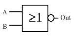
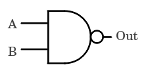
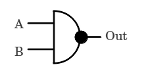
News The Project Technology RoboSpatium Contribute Subject index Download Responses Games Gadgets Contact <<< Function generator Computer >>> Logic gatesThe video about logic gatesData interpretationWhenever sensors are acquiring data, the main intention is to get an interpretation of the sensor output. A simple kind of analysis is done by a twilight switch consisting of a photo sensor and a Schmitt trigger. There is no need to read the current value of the photo sensor, but the question is if there is already enough ambient light, so that the lamp can be turned off, saving valuable electric energy. On the other hand the lamp should be turned on whenever it is getting too dark to see. To make the lamp control more energy efficient, another condition can be added before the lamp is turned on: There is no need to turn the lamp on if nobody is close to it. A motion detection can be integrated as a second sensor to the layout of the circuit. The lamp should be turned on, if it is dark AND if somebody is close to it. On the other hand, the lamp should be turned off, if nobody is close to it OR if the sun is shining. Logic gates are used to trigger a device into operation by more than one enabling signal.AND gate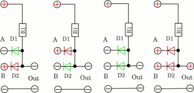
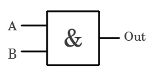
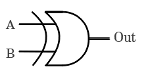
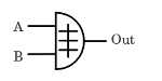
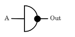
A simple AND gate composed of two diodes an one resistor was introduced at the chapter about H bridges: The signal at the output terminal of the circuit is LOW whenever one of the input signals is low, because the potential is kept at ground level by the forward biased diode(s). The output is HIGH if both input terminals are HIGH, because both diodes are reverse biased and the potential at the output clamp is kept at high level by the pull-up resistor. OR gate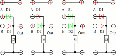
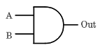
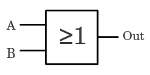
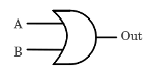
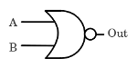
The output of an or gate is HIGH, whenever at least one of the inputs is HIGH. If neither input is HIGH, the resulting output is kept at low level by the pull-down resistor. XOR gate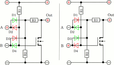
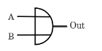
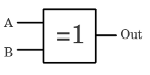
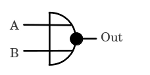
The XOR gate implements an exclusive OR. The output is HIGH if only one of the inputs is HIGH. At the left of the drawing, input A is HIGH, hence D1 is forward biased and the drain voltage of the transistor equals (nearly) the potential at input A, which is the supply voltage. Input B is LOW, hence D4 is also forward biased, pulling the base of the transistor to (nearly) zero volts. The transistor is turned off, hence the potential at the output terminal equals (nearly) those of input A which is the supply voltage. At the right of the drawing, input A is LOW, while input B is HIGH. Now the drain voltage of the transistor is provided by input B, while the gate of the device is pulled to ground by input A. 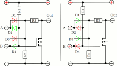
If both inputs are LOW, D2 and D4 are forward biased, pulling the gate of the transistor to ground, hence the device is turned off. D1 and D3 are reverse biased, hence the drain voltage and so the output terminal is pulled to ground via R2 and R3. If both inputs are HIGH, D2 and D4 are reverse biased, hence the gate voltage of the transistor is pulled to (nearly) the supply voltage by R1, hence the device is turned on. The resulting drain voltage and so the potential at the output terminal is (nearly) zero volts. NOT gate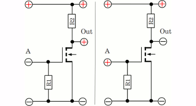
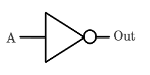
The NOT gate is a simple inverter. There is just one input terminal and the output signal is HIGH when the input is LOW and vice versa. NOR gate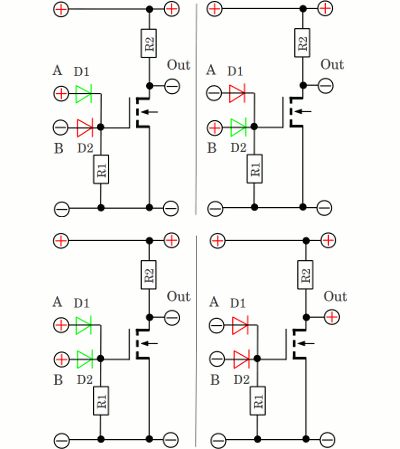
When inverting the output of an OR gate, the resulting circuit is a NOR gate (Not OR). A HIGH output results if both inputs to the gate are LOW. Any other input combination results in a LOW output. NAND gate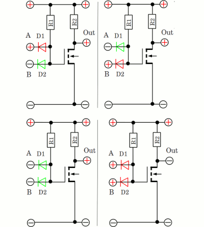
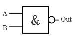
When inverting the output of an AND gate, we get a NAND gate (Not AND). The output of the NAND gate is LOW only if the two inputs are HIGH. If one or both inputs are LOW, a HIGH output results. Ideal versus real logic gatesThe output of an ideal logic gate can be either zero volts or the supply voltage. If the output equals zero volts, the state is also called LOW, 0 or FALSE. On the other hand if the output equals the supply voltage, the state is called HIGH, 1 or TRUE. No current is running through the inputs of an ideal gate, while the output impedance is zero. The propagation delay, which is the length of time taken for the quantity of interest to reach its destination, is zero. No time passes by until the signal travels from the input(s) to the output of the gate.There are a few drawbacks to the discrete logic gates drawn above: When the output signal is LOW, the voltage drop is different from zero. For example those of the AND gate equals the voltage drop across a forward biased diode, which is usually 0.6V when using silicon types. On the other hand, the output voltage is 0.6V from the supply voltage if the output is HIGH at the OR respectively the XOR gate. The AND respectively OR gates are passive, hence the output drive is limited. The "inner resistance" of the AND gate is caused by R1, while those of the OR gate depends on the inner resistance of the input signal. Integrated circuits are the better choice than discrete circuits and there is a large number of different chips available on the market: The output HIGH respectively LOW voltage is very close to the supply voltage respectively to zero volts. The difference is usually 0.05V and below. There is sometimes a Schmitt trigger at the input terminals, hence the output is indeed either HIGH or LOW and the impact of noise is reduced. The gates are active (even the OR respectively AND gates), hence a large number of gates can be wired in series or in parallel with one another. The input leakage current is just some μA. Truth table / circuit symbols
Universal logic gatesNAND gates or alternatively NOR gates alone can be used to reproduce the functions of all the other logic gates. A NOT gate is made by joining the inputs of a NOR respectively NAND gate. The drawing shows the construction of a NOT, OR, AND respectively a XOR gate by using NAND gates at the left, NOR gates at the right side. A XNOR gate can be built by adding a NOT gate to the output of a XOR gate.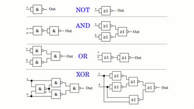
Logic gates can be constructed by using one of several different designs with compatible logic levels and power supply characteristic. A group of electronic logic gates using identic construction principles is called logic family. Resistor diode logic RDL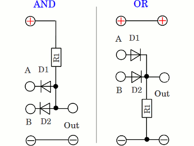
By using resistor diode logic, the only functions which can be built are OR respectively AND gates. The working principle is described above. The advantage is the simplicity of the design, but the lack of an amplifying stage makes it nearly impossible to cascade RDL gates. Resistor transistor logic RTL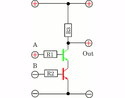
Resistor transistor logic is a class of circuits using resistors at the input network and bipolar junction transistors at the output. If the input at one of the transistors is LOW, the accordant device cannot conduct, hence the output signal is HIGH. The only way the output can be LOW is if both transistors are turned on by a HIGH level at the inputs. It is a NAND gate. 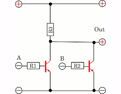
The NOR gate consists of a set of parallel-connected transistor switches driven by the logic inputs. Diode transistor logic DTL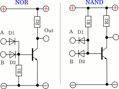
The logic gating function of DTL circuits is performed by a diode network while the amplifying function is performed by a transistor. The working principle of a NAND respectively NOR gate is described above. Transistor transistor logic TTL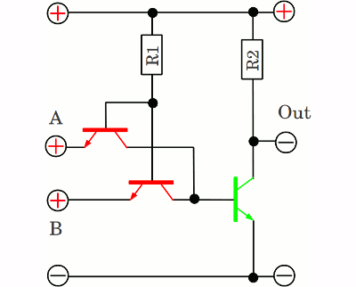
The logic gating function and the amplifying function of TTL circuits are performed by bipolar junction transistors. The output impedance of this simple TTL NAND gate depends on the value of R2. The lower the resistance value, the lower the impedance of the gate while the output is on HIGH level, but the higher the current running through the device while the output is on LOW level. 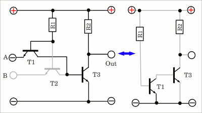
If there is a LOW signal at one of the inputs, the circuit is equal to that on the right of the animated drawing: The emitter is connected to ground, while the base is connected to the positive supply voltage via resistor 1. The collector is connected to the base of transistor 3. The transistor is turned "on", which is why almost no voltage is applied to the base of transistor 3, hence that device is turned "off" and the output signal is HIGH. 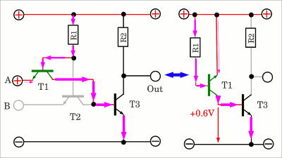
If there is a HIGH signal at the input, the emitter gets connected to the positive supply voltage. The potential at the collector pin won't exceed 0.6V, because the emitter base diode of transistor 3 becomes conductive at higher values. The equivalent circuit diagram is a transistor operating in reverse mode, whose base is connected to the positive supply voltage via resistor 1. The current running through the base of transistor 1 causes two effects: On the one hand that current also runs through the base of transistor 3 and on the other hand the current turns the collector emitter line of transistor 1 "on". Both effects make the emitter collector line of transistor 3 conduct, hence the output signal becomes LOW. Like explained in the video about the properties of bipolar junction transistors, the current gain in reverse mode is clearly lower than in normal operation. Otherwise the input current would increase dramatically and transistor 3 would be damaged because of a too high base voltage respectively a too high current. 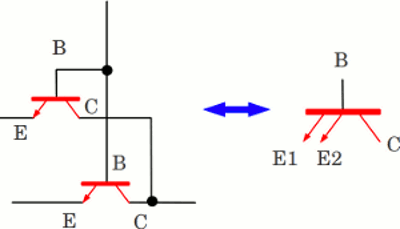
At the NAND logic gate described above, the base and collector terminals of the transistors at the inputs are joined together. To get a more compact design, multiple-emitter transistors are used instead when constructing a packaged IC die. Those specialized bipolar transistors have a single collector respectively base area, with separate emitter areas. Collector current stops flowing only if all emitters are driven by the logical high voltage, thus performing an AND logical operation using a single transistor. 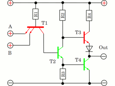
By adding a push-pull output to the gate, the problem with the high output resistance can be solved: Whenever T1 is turned "off", T2 is turned "on", by what T4 is activated, driving LOW voltage to the output. The potential at the base of T3 is just slightly higher (approximately 0.2V) than those at the base of T4. To turn T3 reliably "off", a diode is placed between the collector of T4 and the emitter of T3. Now the potential at the emitter of T3 is approximately +0.8V (0.6V + 0.2V) and the resulting base voltage is clearly below 0.6V. When T1 is turned "on", T2 and T4 are turned "off" and T3 operates in active region as a voltage follower producing high output voltage. When neglecting the resistance of T3 and the forward biased diode, the output resistance of the gate depends on the value of R4, which equals R2 at the simple circuit. The advantage of the "push-pull" output is that even if the resistance value of R4 is very low, (almost) no current is running through the leg composed of R4, T4, the diode and T3, neither if the output is HIGH and no load is connected to the output nor if it is LOW. R4 also limits the current in the middle of the transition while T3, T4, and the diode are conducting (shoot through) or in case there is a short connection to ground while the output is HIGH. The output stage is also called totem-pole. A disadvantage of the circuit is the decreased voltage level of the output logical "true" caused by the voltage drop across the emitter-collector line of T3 and the forward biased diode. 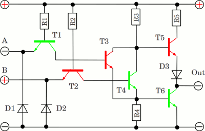
TTL double input NOR gate with totem-pole output: The functionality is easy to understand while remembering that there are two p-n junctions inside of a bipolar junction transistor. If input A is on HIGH level, the p-n junction between base and collector of T1 becomes forward biased, hence a current is running through R1 and so through the base of T3, turning this device "on". If input A is LOW, T1 is functioning as a normal amplifying stage: There is a current running through the base of T1, bringing the device into saturation. While T1 is turned "on", the base of T3 is pulled to ground, hence this device is turned "off". D1 and D2 prevent prevent negative voltage spikes at the inputs of the circuit. Complementary metal-oxide-semiconductor logic (CMOS)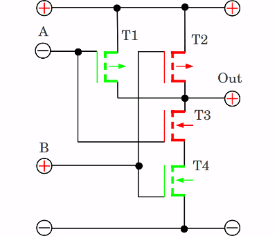
Circuit diagram of a NAND gate in CMOS logic: If input A and B are HIGH, neither of the p-channel MOSFETs (T1 and T2), but both n-channel MOSFETs (T3 and T4) will conduct, hence a conductive path is established between the output and ground, bringing the output LOW. If either input A or B is LOW one of the p-channel MOSFETS will conduct, while one of the n-channel MOSFETs wont. A conductive path is established between the output and the positive supply voltage, bringing the output HIGH. If both inputs are LOW, the two n-channel MOSFETs are turned "off", while the p-channel MOSFETs are turned "on". Once again there is a conductive path between the output and the positive supply voltage, while none of the n-channel MOSFETs between output and ground conducts. 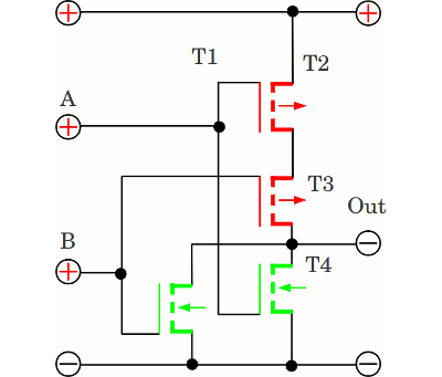
Circuit diagram of a NOR gate in CMOS logic: The functionality is very similar to those of the NAND gate. Each input is connected to the gate of one n-channel and one p-channel MOSFET. In contrast to the NAND gate, the two n-channel MOSFETs are switched in parallel, while the p-channel types are switched in series. <<< Function generator Computer >>> News The Project Technology RoboSpatium Contribute Subject index Archives Download Responses Games Links Gadgets Contact Imprint |
||||||||||||||||||||||||||||||||||||||||||||||||||||||||||||||||||||||||||||||||||||||||||||||||||||||
|
|