|
|
|
|
News The Project Technology RoboSpatium Contribute Subject index Download Responses Games Gadgets Contact Function generatorThe video about function generatorsWaveforms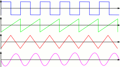
A device used to generate different types of electrical waveforms over a wide range of frequencies is called function generator. The most common wave forms are square, sawtooth, triangular or sine wave shapes (drawn from top to bottom). Triangular shape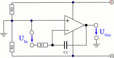
The drawing shows an integrator circuit. There is a negative feedback provided by the capacitor, hence the potential at the inverting and the non inverting input is held equal by the operational amplifier. The non inverting input is connected to ground, while the inverting input is connected to the input clamp of the circuit through R1. 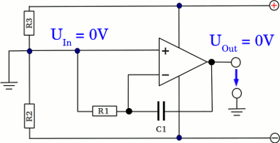
If the input clamp is connected to ground, the difference in potential between the inverting and the non inverting input is zero volts, hence the resulting output voltage of the operational amplifier is zero volts, too. Both plates of the capacitor are at the same potential. Furthermore both sides of the resistor are at the same potential, hence no current is running through the device and the state of the circuit is stable. 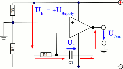
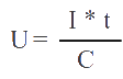
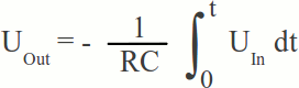
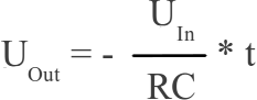
If the input clamp of the circuit is connected to the positive supply voltage, the capacitor gets charged via R1, hence the potential at the inverting input would increase, but caused by the negative feedback, the voltage at the output clamp of the operational amplifier is decreasing in such a way, that the potential at the inverting input is kept at those of the non-inverting input, which it the ground level. While the left side of R1 is connected to the positive supply voltage and the right side of R1 is kept on ground by the operational amplifier, the voltage drop across the device and so the current through R1 and C1 is constant. For the relation between charge and a constant current there is (see chapter about current for details): Furthermore, at the chapter about capacitors, the relation between between cumulated charge and voltage was discussed: So for the voltage across the capacitor over time there is: Where is: U - voltage across the capacitor I - current through the capacitor C - capacitance t - time There is a linear correlation between the voltage across the capacitor and the time passing by. Remember that the current and the capacitance are constant values. To keep the inverting input on ground level, the output voltage of the operational amplifier is counterbalancing the increasing potential across the capacitor and there is: UOut = -UCapacitor 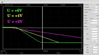
Oscillograph plot of the output voltage: The higher the (constant) input voltage, the higher the current through the resistor, hence the higher the (negative) slope of the straight line. Derived from [9.5], there is also a linear correlation between the slope and the resistance of R1 respectively the capacitance of C1. When doubling the resistance of R1 or the capacitance of C1, the slope of the curve gets halved. The output voltage of the operational amplifier can't exceed the input voltage, hence, after a fixed span of time the negative supply voltage is reached. 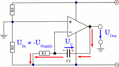
If the input clamp of the circuit is connected to the negative supply voltage, the capacitor gets charged with reverse polarity. The voltage at the output of the operational amplifier is increasing to keep the potential at the inverting input on ground level. 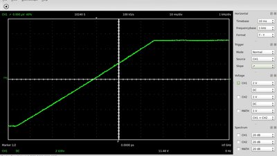
Starting with the negative supply voltage, the potential at the output clamp of the operational amplifier is now increasing until the positive supply voltage is reached. 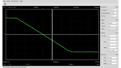
If the input voltage tilts back to the negative supply voltage, the output voltage is decreasing until the negative supply voltage is reached again. The intention is to get a triangular curve progression, so all we have to do is altering the input voltage of the circuit from the positive to the negative supply voltage whenever the output voltage is close to the negative supply voltage respectively altering the input voltage from the negative to the positive supply voltage whenever the output voltage is close to the positive supply voltage. A circuit suitable for that is a Schmitt trigger: 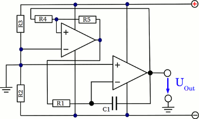
The output signal of the integrator is connected to the input clamp of the non inverting Schmitt trigger (left operational amplifier). The output of the Schmitt trigger, which is connected to the input of the integrator, tilts to the positive supply voltage, whenever the output of the integrator reaches the upper threshold. Now C1 gets charged with reverse polarity, until the output of the integrator reaches the lower threshold. Now the Schmitt trigger tilts to the negative supply voltage, which is why the output voltage of the integrator is increasing again. 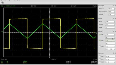
Signal at the output clamp of the circuit (green curve) and at the output of the Schmitt trigger (yellow curve) which is the input of the integrator. 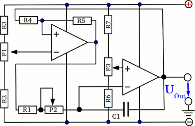
When inserting three potentiometers, the shape of the output curve can be varied. Potentiometer number one alters the lower and upper threshold of the Schmitt trigger, hence the level of the output curve can be adjusted by this device. Potentiometer number two enables the adjustment of the frequency. Like explained above, the charging respectively discharging current is higher the lower the resistance of P2, hence the slope of the curve and so the frequency is increasing. Potentiometer number three is for the adjustment of the symmetry. 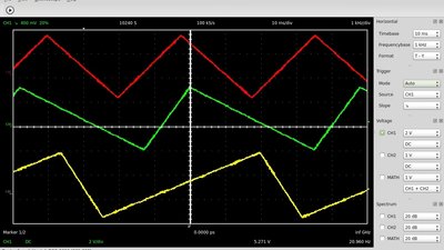
The reference potential of the integrator is varied by P3. The output voltage of the Schmitt trigger is either the positive or the negative supply voltage. If the reference potential of the integrator is close to the positive supply voltage, there is a low difference in potential between the input and the reference voltage, hence the current through C1 and so the slope of the output curve is also low. In contrast, if the signal of the Schmitt trigger tilts to the negative supply voltage, there is a high difference in potential between the input and the reference potential at the integrator, hence the slope of the curve is high while the capacitor gets charged with reverse polarity (green curve). If the reference potential is adjusted to half the value of the difference between positive and negative supply voltage (which is ground at the previous examples), the curve progression is symmetrically (red curve). Sawtooth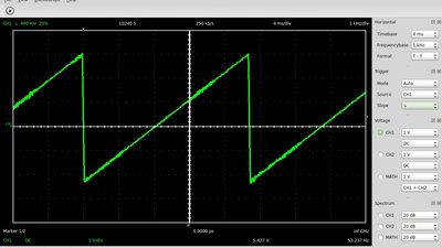
A sawtooth signal is in principle a triangular signal with a relatively slow linear ramp and a rapid fall at its end. 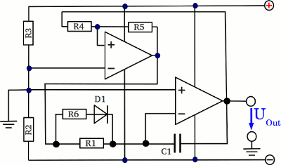
R1 and R6 are switched in parallel. By inserting a diode in series to R6, the total resistance of the combination depends on the polarity of the voltage. While the output voltage of the Schmitt trigger equals the negative supply voltage, D1 is reverse biased, hence the charging current of C1 is running through R1. If the output voltage of the Schmitt trigger tilts to the positive supply voltage, D1 becomes forward biased, by what the current running through C1 is clearly higher while the device is charged with reverse polarity. The fall time of the signal is clearly lower than the rise time. R6 should be as low as possible - consider the maximum current of the operational amplifier. Square wave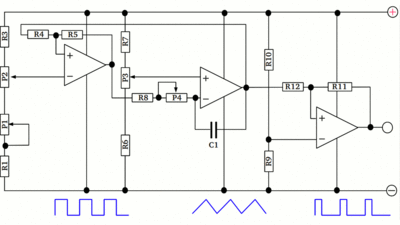
An astable multivibrator generates a square wave signal. With the knowledge about the integrator circuit discussed above, the working principle of the circuit introduced some chapters before should be easy to understand. Sinusoidal signalMore generally speaking the voltage-current relationship of a capacitor is governed by the equation:Furthermore the relation between the resistance of R1 and the current through the device and so through the capacitor is given by:
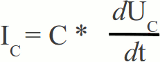
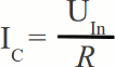
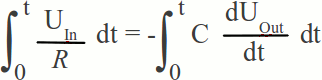
UOut = -UC Integrating both sides with respect to time:
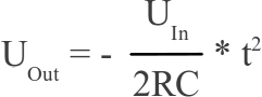
UC - voltage across the capacitor IC - current through the capacitor C - capacitance t - time UOut - output voltage of the integrator circuit UIn - input voltage of the integrator circuit R - constant resistor The output voltage is proportional to the input voltage over time: The circuit performs the mathematical operation of integration with respect to time. Assuming that the capacitor was discharged while t=0 and that UIn is kept constant, [9.7] can be transformed to: Which is the function of a straight line. If the input voltage is a square wave signal, the resulting output of the integrator circuit is the triangular voltage shown above. The integration of [9.8] over time results in: Which is a quadratic function if UIn is constant and something looking very similar to a sine wave when using the square wave signal as input: 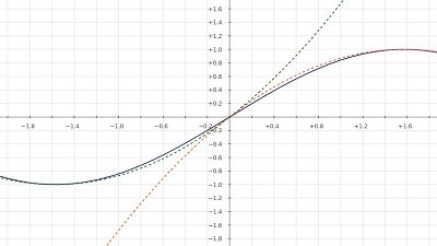
The blue curve is a sine wave, the red and green curve are quadratic functions being as close as possible to the sine curve. When switching two integrator circuits in series and connecting the input of the first one to a square wave signal, we get an output voltage which is very similar to a sine wave: 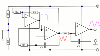
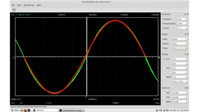
Oscillograph plot of the "sine wave" (green curve) at the output clamp of the function generator compared with an ideal sine wave (red curve). Differentiator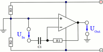
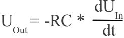
When swapping C1 and R1, the resulting circuit is called active differentiator. The negative feedback loop is now running via R1 while C1 is used at the input side. Caused by the negative feedback, the potential at the inverting input of the operational amplifier is kept on virtual ground, hence the input voltage equals the voltage across the capacitor, while the voltage across the resistor equals the output voltage (except the sign) and there is: UC = -UOut The current to voltage relationship of a capacitor is given by [9.6], while those at the constant resistor is given by [3.7]. Rearranging the equations results in: Where is: UIn - input voltage of the differentiator UOut - output voltage C - capacitance R - resistance The output voltage is proportional to the time derivative of the input, hence the circuit acts as a differentiator. Test boardLayout of the board used in the video (click to enlarge):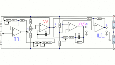
Operational amplifier = MC34074P R1, R2, R3, R5, R6, R7, R10 = 1kΩ R4 = 12kΩ R8, R9 = 2.7kΩ R11, R13 = 1MΩ R12 = 33kΩ P1, P2, P4, P5, P6 = 10kΩ P3 = 100kΩ C1 = 0.33μF C2 = 0.1μF To avoid feedback between the output 1-4 and a load connected to the board, four additional operational amplifiers should be inserted. For example connecting a differentiator with a capacitor at the input terminal directly to the triangular signal of the board, will result in oscillations at certain frequencies: 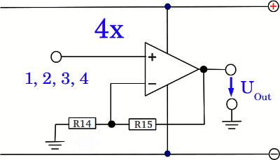
R13 = R14 = 1MΩ A second operational amplifier type MC34074P or high power devices can be inserted to get a high output current (z.B. two L272 Chips). In the video, a single battery served as voltage source and the mid point of a simple voltage divider (R8, R9) was used as ground level. If your intention is to connect a load with a low resistance (e. g. a loudspeaker) to the output of the frequency generator, a symmetrical power supply is required. You can use two identical batteries instead. 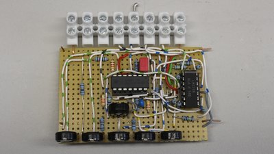
The function generator is definitely not perfect. For example, whenever the amplitude of the triangular signal is varied, the frequency of the output signal alters, too. Whenever one parameter is varied, the other parameters have to be readjusted. Nevertheless the board is suitable for demonstration purposes. The frequency rage is approximately 25Hz - 1kHz. If higher frequencies are required, C1 and C2 have to be replaced by devices with a lower capacitance. The used operational amplifier sets the limit. Simply try it out and mail your own results. News The Project Technology RoboSpatium Contribute Subject index Archives Download Responses Games Links Gadgets Contact Imprint |
|
|