|
|
|
|
News The Project Technology RoboSpatium Contribute Subject index Download Responses Games Gadgets Contact ComputerThe video about calculating machinesBinary numberThe binary system is used internally by almost all computer-based devices. A binary numeral system, or base-2 numeral system, represents numeric values using just two symbols: 0 and 1. In contrast the decimal system uses ten symbols 0, 1, 2, 3, 4, 5, 6, 7, 8, and 9. When doing counting, the low-order digit, which is the rightmost digit is incremented by one. If the low-order digit in the decimal system is 9, the next-higher-order digit, located one position to the left is incremented and counting in the low-order digit starts over at 0. For decimal counting we get:001, 002, 003, ... 008, 009, 010, 011, 012, 013, ... 018, 019, 020, ... 091, 092, 093, ... 098, 099, 100, 101, 102, 103, ... 198, 199, 200. 
Binary counting follows exactly the same rules, except that only two symbols are available, hence after a digit reaches 1 in binary, counting starts over at 0 while the next-higher-order bit is incremented. Each digit of a binary number represents an increasing power of 2, with the rightmost digit representing 20, the next representing 21, then 22, and so on. The rightmost digit is also named Least Significant Bit, LSB, while the leftmost digit is named Most Significant Bit, MSB. In computing, a binary digit is named bit and it is the base unit of information. A byte is a unit of digital information in computing that most commonly consists of eight bits. One byte can store 28 = 256 different binary values, usually representing the numbers 0 to 255: 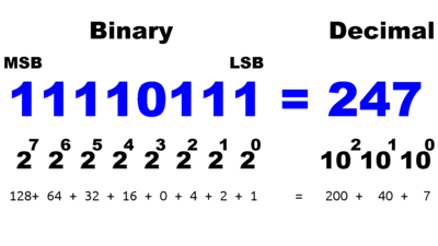
Data storageA bit can be implemented in electronic circuits by a two-state device like a latch. Besides using discrete devices, a latch can also be constructed from a pair of cross coupled NOR logic gates: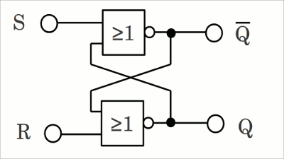
SR NOR latch. 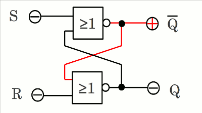
Whenever the circuit is connected to the supply voltage, the initial state depends on the electric properties of the logic gates. The output signal at Q can be either HIGH or LOW. Let's assume the signal is LOW. The input signals S and R are also LOW. Both inputs at the upper NOR gate are LOW, hence the output signal of the gate is HIGH. The output of the upper gate is connected to one of the inputs of the lower one, hence one of the inputs of that gate is HIGH and so it's output signal is LOW. The state of the whole circuit is stable. Q is HIGH, bringing the cross coupled gate of Q LOW, which in turn keeps the upper gate of Q HIGH. 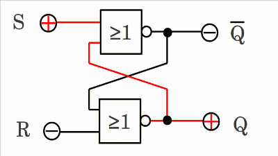
If input S is connected to HIGH level, the state of the circuit changes: The output of the upper gate changes from HIGH to LOW level, hence by now both inputs of the lower NOR gate are LOW. The output of the lower gate changes to HIGH level, by what both inputs of the upper gate are HIGH. The state of the circuit is stable. Q is HIGH, while Q is LOW. 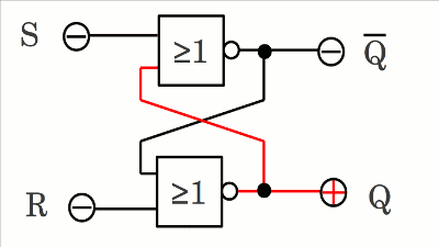
If input S falls back to LOW level, the feedback maintains the output state. While both inputs are LOW, the circuit is in hold state. 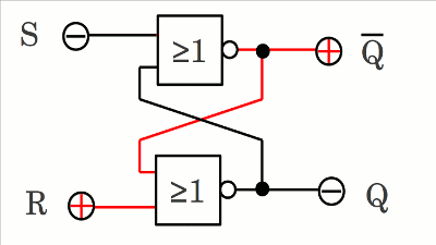
If R is connected to HIGH while S is held LOW, the Q output changes from HIGH to LOW, forcing the upper gate to change from LOW to HIGH via the cross coupled input. 
Output Q maintains LOW level during hold state. Input S is called Set, bringing output Q to HIGH, while input R is called Reset, bringing Q to LOW. Output Q is the complement of Q (Q = NOT Q). 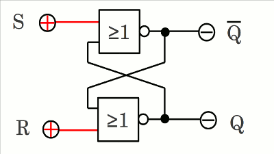
If both inputs are HIGH, the combination is called forbidden state or restricted combination. Both outputs Q and Q are LOW and the logical equation Q = NOT Q is broken. During normal operation of a single storage cell, this state should never occur. 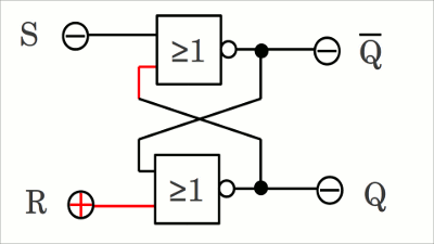
Animated drawing of a NOR SR latch. 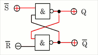
Animated drawing of a NAND SR latch. When using two cross coupled NAND logic gates, Set and Reset become active LOW signals, denoted S respectively R. S = LOW, R = HIGH sets the output Q HIGH. S = HIGH, R = LOW sets the output LOW. S = HIGH, R = HIGH is the hold state. S = LOW, R = LOW is the restricted combination. 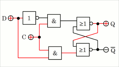
By inserting additional logic gates to the inputs of the NOR SR latch, the resulting circuit is named gated latch. If input C (Control, Clock) is LOW, the output of both AND gates is also LOW, hence the input of the SR latch is in hold state. If C switches to HIGH, the gate becomes transparent and the state of input D (Data) propagates directly through the circuit to output Q. The output is set whenever input D is HIGH and it is reset if D is LOW. The C input is sometimes denoted by an E (Enable). The configuration of the gated D-latch prevents the application of the restricted input combination. 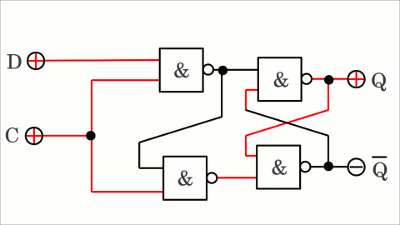
Two additional NAND gates are required to turn the NAND SR latch into a gated SR latch. The input NAND stage inverts the data input signal, hence the LOW state of the control signal produces the hold state at the input of the SR latch (HIGH signal at both inputs). Caused by propagation delay, the restricted combination (LOW signal at BOTH inputs of the SR latch) can be observed for a short span of time at the animated drawing. Furthermore the output of Q equals Q temporarily. Even if this drawing isn't an exact description of the processes inside of a gated latch, you should consider that the propagation delay of the whole circuit is increasing with each logic gate added to the layout. If your "computer" is operated with too high clock rates, the output of the memory will be scraped. To avoid misinterpretation of the stored data, the read process should not be started while the data signal propagates through the circuit. 
Three SR NAND latches are required to build a positive-edge-triggered D flip-flop. Whenever the control input is LOW, both inputs of the output latch to the right are HIGH, regardless of the data input, hence the output latch is in hold state, storing the previous state. Depending on the data signal, Q is SET or RESET when the control signal changes from LOW to HIGH. Even if the control input stays high, the output Q keeps its state regardless of the data input. The positive-edge-triggered D flip-flop captures the value of the data input at the rising edge of the control signal. Depending on the propagation delay, some time passes by until the data signal crosses the circuit to the output. 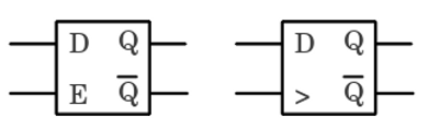
Latches are available as integrated circuits, usually with multiple latches per chip. The left symbol shows a gated D latch, the right a positive edge-triggered D flip-flop. RegisterTo be able to store more than just a single bit, several flip-flops have to be grouped. If the flip-flops are arranged in a chain, sharing the same clock and with the output of one flip-flop connected to the data input of the next one, the circuit is called shift register. All bits of the chain shift by one position at the rising edge of the clock signal.During write operation, each data bit of one byte is presented at the D input connected to the first flip-flop and all bits are shifted right each time the clock signal (C) is rising. After 8 cycles, one byte is stored in a 8 bit register (click at the drawing to start the animation): 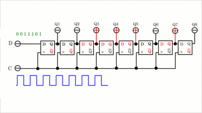
The byte can be read after the write operation is finished in parallel mode at the outputs Q1 - Q8. It has to be ensured that the read operation is not triggered during write operation or else you will get scraped data. To avoid change of the parallel outputs during write operation, a latched output can be added to the circuit (see below). The circuit is a Serial-In, Parallel-out (SIPO) register. While the register is clocked, the stored data can also be read at the output Q8 of the far right flip-flop (Serial-In, Serial-out mode, SISO). With each cycle the bit at that flip-flop is shifted out and lost while a logical 0 is stored at the far left flip-flop, hence it is a destructive readout (click at the drawing to start the animation): 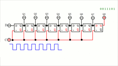
The wiring scheme of a multiple purpose 3 bit register is more complex (click on the image to see the animated version): 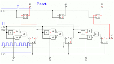
The register can be operated in several modes: With the Load input (L) disabled (LOW), the register operates in serial mode, writing data at the DI input (Data In) into the memory cells and shifting that data with each rising edge of the clock signal to the DO (Data Out) output (SISO). A single pulse at the E (Enable) input copies the state of the shift register into the output register (SIPO) and so to the output pins Q1 - Q3. While the Load input is enabled (HIGH), the state of the inputs D1 - D3 is copied into the shift register as soon as the clock signal is rising. A single pulse of the clock signal is sufficient for the load process. (Parallel-In, Serial-Out PISO). A single pulse at the Reset (R) line clears the memory (all bits are '0'), which is faster than loading triple '0' data in serial mode. The circuit can also be used in Parallel-In, Parallel-Out PIPO mode. Additional flip-flops can be connected to the DO pin to get a larger amount of memory e. g. a total of eight flip-flops results in one byte of storage. MultiplexerA data selector, also called multiplexer, or short mux is a device that selects one of several input signals and forwards the selected input into a single line.With a multiplexer, several signals can share a single device. For example the Atmega8 microcontroller has one built in analog-to-digital converter, but up to 6 pins can be connected to the input line of the converter via a multiplexer. 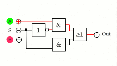
The multiplexer drawn here was used at the register circuit above to select whether the device operates in serial or parallel mode. If the Select (S) signal is LOW, input A is forwarded to the output, while the output signal equals input B whenever the Select signal is HIGH. (Click on the drawing to see the animation.) 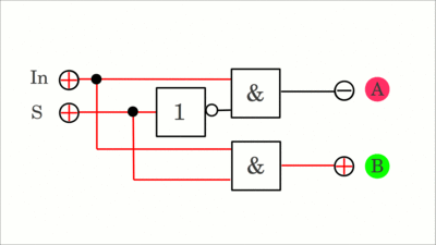
A demultiplexer or short demux takes a single input signal and selects one of many output lines. At the circuit drawn here, the signal at the input line is forwarded to output A, whenever the Select (S) signal is LOW. Output B is chosen if the Select signal is HIGH (Click on the drawing to see the animation). The disabled output stays on LOW level. With a multiplexer, one out of several inputs can be sent to a single data line while the demultiplexer can be used to forward the data to one of several outputs (click on the drawing to see the animation): 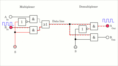
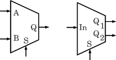
Circuit symbols for a 2-to-1 multiplexer (left) and a 1-to-2 demultiplexer (right). CounterThe JK flip-flop is similar to the SR latch discussed before. If the J input is HIGH while the K input is LOW, output Q "jumps" to HIGH level. If the J input is LOW while the K input is HIGH, output Q is "Killed". There is no change in output while both inputs are LOW (hold state). If both inputs are HIGH, the output toggles, hence it changes to the logical complement of the current state.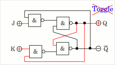
This simple circuit is useful to demonstrate the "jump", "kill" and "hold" functionality, but it fails while trying the "toggle" state. Click at the drawing to see the animated version. The circuit drawn below captures the values of the J and K input while input C is HIGH and the outputs are set at the falling edge of the clock signal. If J=K=HIGH, the output toggles with each clock cycle (click on the drawing to see the working principle): 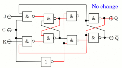
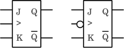
The left of the drawing shows the circuit symbol for a positive-edge-triggered JK flip-flop, the right one for a negative edge triggered version. 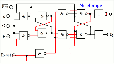
JK -Flipflop with "not set" and "not reset" inputs. If "not set" is on LOW, output Q is forced to HIGH. If "not reset" is on LOW, output Q is forced to LOW. Both inputs must be on HIGH level during operation and should never be on LOW simultaneously. There are two additional buffers on the outputs of the circuit that are not needed for operation, but are often inserted to seperate the output signals from the input signals. 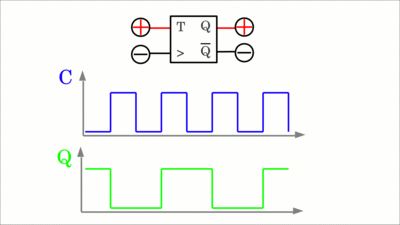
When joining the J and K input, the resulting circuit is a T flip-flop. If the T input is LOW, the flip-flop holds the previous value, while it toggles whenever the clock input is strobed and the input is HIGH. The toggle flip-flop divides the clock frequency by two. Click on the drawing to see the animation. 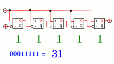
Arranging several negative-edge triggered T flip-flops in a chain with the Q output of one flip-flop connected to the clock input of the next device results in a binary counter. The input signal is connected to the C input of the flip-flop at the far left and all T inputs are connected to HIGH signal. With each falling edge of the input signal, the binary number is increased by one. Even though the animated gif (click at the drawing to start) implements that all flip-flops are switched simultaneously with the falling edge of the input signal, there is a small propagation delay caused by each device in the chain. The transitions of the flip-flops are asynchronous, hence the circuit is an asynchronous counter which can count to 2n- 1 where n is the number of flip-flops. Note that the lowest bit of the binary number is stored in the far left flip-flop. 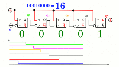
The propagation delay of each flip-flop is added up in the chain of an asynchronous counter while the clock signal crosses the circuit to output Q5. The animation (click on the drawing) shows the transition from 01111 (decimal 15) to 10000 (decimal 16). The output bits "ripple" in sequence from the left to the right, which is why the circuit is also named ripple counter. Keep in mind that the Least Significant Bit at the drawing is on the left and the Most Significant Bit on the right, while binary numbers are usually noted with the LSB on the right. In the time period that the "ripple" takes place, the false outputs 01110 (decimal 14), 01100 (decimal 12), 01000 (decimal 8) and 00000 (decimal 0) are generated. Since the ripple happens very quickly, the effect is tolerable for many applications. The ripple takes place at the falling edge of the clock signal, hence a simple solution to avoid reading wrong outputs is to trigger the read process at the rising edge of the clock signal. 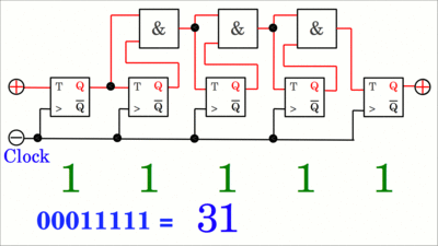
To create a synchronous counter, the external clock signal has to be connected to the clock input of every flip-flop within the counter, hence all flip-flops will toggle simultaneously with the rising edge of the external signal. By inserting AND gates, each flip-flop can be enabled to toggle weather or not the outputs of all preceding flip-flops are on HIGH level. At the drawing (click to start the animation), flip-flop number one on the far left toggles with each rising edge of the external clock signal, while number two toggles only if number one is logic HIGH. Number three toggles if flip-flop one AND flip-flop two are logic HIGH, which is ensured by the AND gate on the far left and so on. Finally flip-flop number five on the far right, representing the most significant bit, toggles only if the four preceding flip-flops are logic HIGH, which is ensured by the three AND gates inside of the circuit. 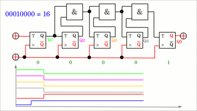
The animation (click on the drawing) shows the transition from 01111 (decimal 15) to 10000 (decimal 16). The outputs of all five flip-flops change simultaneously, hence the total propagation delay of the counter circuit equals that of a single flip-flop and there is no ripple effect. The propagation delay of the AND gates doesn't affect the propagation delay of the counter's output signals, but the maximal frequency of the external clock signal. The next cycle should not start before all gates have reached their final state according to the output of all flip-flops. AdderAdding two values, usually binary numbers, is a very common operation done by computers. When adding two single binary digits the possible result are:
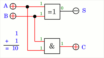
The operation can be implemented by using an AND gate and a XOR gate (click on the drawing to start the animation). Two single binary digits A and B are added and the result is stored in the outputs S (Sum) and C (Carry). The carry signal represents an overflow into the next digit. The decimal value of the sum is The storage of a computer is always limited. A one bit register can store 21 = 2, an eight bit register 28 = 256 different binary values. If a calculation produces a result that is greater in magnitude than that which a given register can represent, the overflow condition occurs. The result of case number 4 is a two bit number while both summands are one bit numbers. 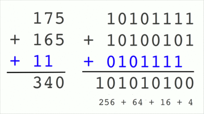
Addition can be done by writing one number below the other and then add one column at a time starting with the right most column. If the result of the partial addition produces an "overflow", meaning the result is a two digit number, the higher digit is carried to the next column. This method works not only for decimal, but also for binary numbers (click at the drawing to see the animation). When adding two binary numbers following the carry method, up to three single bit numbers have to be added at a time. The possible results are:
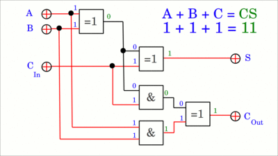
An electronic circuit reproducing the addition of up to three one-bit numbers is called full adder. When adding two binary numbers, the full adder can carry in the "overflow" of the next less significant stage and carry out the "overflow" to the next full adder representing the next more significant stage. 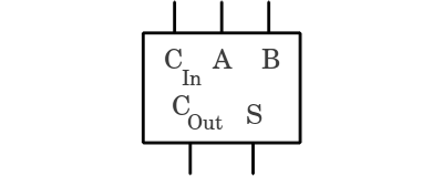
Input A and B of a full adder both represent one-bit binary values. The carry-in input is connected to the carry-out pin of the adder representing the next less significant stage. The circuit produces a two bit output named S (Sum) and COut (Carry-out). Two multi-bit numbers can be added by using multiple full adders arranged in a chain with the CIn connected to the COut of the next less significant stage. A half adder can be used at the least significant stage (rightmost adder at the drawing). Caused by propagation delay, each carry bit "ripples" to the next full adder, which is why the circuit is named ripple-carry adder. Click at the drawing to see the animated version showing the procedure of adding the values 175 and 165. While the ripple takes place, the false outputs 266 and 320 are generated. Note that the carry out bit at the most significant stage is set after the addition procedure has finished, indicating that the result (340) is too large to be stored in an 8-bit register. 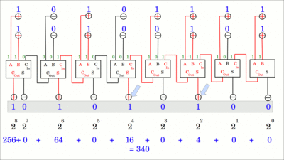
SubtractorWhile the overflow condition might occur when adding two binary numbers, the result of a subtraction may drop below zero. In computing, different data types represent different numbers. An unsigned 8-bit integer can hold values from 0 to 255 inclusively, while a signed 8-bit integer can represent a number between -128 and +127 inclusively. For this sign representation method, the leftmost bit denotes whether the value is positive or negative. The value is negative if the leftmost bit is 1, because the value of the most significant bit is subtracted from the sum of all other bits when converting from the binary into a decimal number: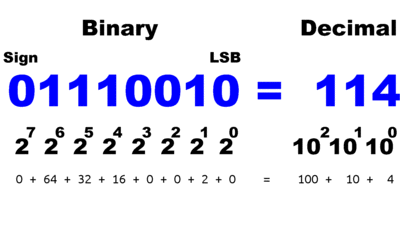
Considering the numerical representation of signed binary numbers above, which is called two's complement, the decimal number +127 becomes the 8 digit binary number 01111111. Inverting all digits and adding 1 results in: 10000000 + 1 = 10000001 which is -127 in decimal system. Remember that the leftmost digit represents the sign of the value which is 1, hence it's a negative value. 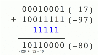
In general each subtraction can be turned into an addition: A - B = A + B + 1 The subtraction of The result of the addition is 10110010 in binary system which complies to -80 in decimal system following the rules of the two's complement. Click on the drawing to see the animated calculation of The ripple-carry adder can be turned into a ripple-carry subtractor by inserting XOR gates at the B-inputs and using a full-adder at the least significant stage. Another XOR gate is connected to the carry-out of the most significant stage (leftmost full-adder). Input M controls the operating mode of the circuit. If M is LOW, the carry-in of the rightmost full-adder is also LOW and the circuit operates in adder mode like explained before. If M is HIGH, the carry-in signal of the rightmost full-adder is HIGH, which adds 1 to the result. One input of each XOR gate is brought HIGH, hence the bits of Register B become inverted at the outputs of the XOR gates. The circuit operates in subtractor mode (click on the drawing to see the animation): 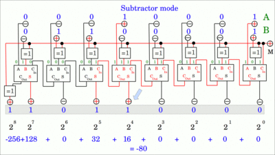
Multiplying can be computed by repeated addition: For example 3 multiplied by 7 is equal to adding seven copies of 3: 3 * 7 = 3 + 3 + 3 + 3 + 3 + 3 + 3 = 21 Consider the overflow condition after each addition! Multiplying 17 with 100 reaches overflow after 16 cycles when using 8-bit unsigned integer values: 17 * 15 = 255, 17 * 16 = 272 Certain division algorithms can also be implemented by using addition respectively subtraction methods. Dividing two integers may result in a remainder ("left over"), which leads to another class of numerical values in computing: Floating point numbers, representing an approximation of a real number. Using the wrong type of number for a mathematical operation is a very common source of error when writing computer software. Creating your own circuitsI used integrated logic gates to create the demonstration circuits in the video. The maximum current of the LEDs used to visualize the logical state of the inputs/outputs is approximately 30mA. Since the maximum output current of the logic gates is below that value and one output drives usually more than just one input, I used 560Ω series resistors to limit the current. When operating the circuits with 5V supply voltage, the current is below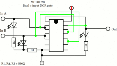
The NOR gates are based on a CD4002BE chip. The green lines are optional, joining the inputs/outputs of the first and the second NOR gate on the chip to get a higher output current. 
The AND gates are based on a HFC4082BE chip. 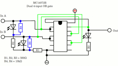
The OR gates are based on a CD4072BE chip. 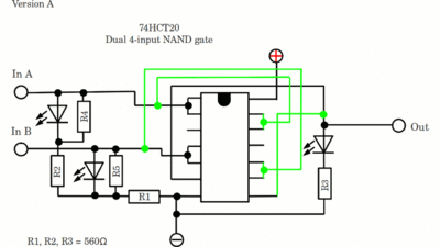
The NAND gates are based on a CD74HTC20 chip. I had some trouble with the LOW level, hence I placed 13kΩ resistors in parallel to the yellow LEDs at the inputs. Version A: The series resistor / LED combination is switched in parallel to the inputs of the gate, hence the HIGH level is equal to the supply voltage (5V). 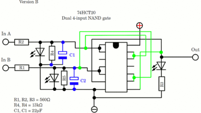
Version B: Only the LED is switched in parallel to the inputs of the gate, the series resistor (R1 respectively R2) isn't, hence the HIGH level is equal to the voltage drop across the LED. The advantage is that a low-pass filter can be easily implemented by inserting capacitors in parallel to the yellow LEDs at the inputs (see edge triggered flip-flop in the video). 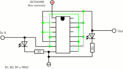
The NOT gates are based on a HCF4009B chip. The green lines are optional, joining the inputs/outputs of all NOT gates on the chip to get a higher output current. Since the output current of this device is very low, the green lines should be soldered. News The Project Technology RoboSpatium Contribute Subject index Archives Download Responses Games Links Gadgets Contact Imprint |
|
|