|
|
|
|
News The Project Technology RoboSpatium Contribute Subject index Download Responses Games Gadgets Contact <<< Pulse-width modulation H bridge >>> Constant voltageThe video about constant voltageIdeal versus real world voltage sourceAn ideal DC voltage source supplies a constant potential between it's terminals for any current flow through it - however we are not living in an ideal world, but our intention is to get as close to it as possible. Let's discover the properties of a 12V rechargeable Battery: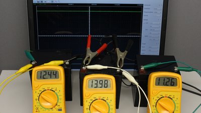
The nominal voltage output of the battery is 12V, but almost each time you connect a voltmeter to the terminals of the battery, you will detect a value being at least slightly different from those 12V. The chemical processes generating the voltage output are dependent from the concentration of certain ions inside of the battery. The concentration fluctuates whenever the battery gets discharged respectively charged. The end of charge voltage and so the maximum voltage should not exceed 14V and you should stop discharging the battery when a potential of 11.2V is reached. There is another property of batteries which has to be considered when a constant voltage is required for your application: The current-voltage characteristic while connecting a load to the battery. Let's assume the voltage drop with no load connected to the battery is 12.5V. When attaching a 12V 10W filament lamp to the terminals, the potential is decreasing to just 12.3V. A current of approximately 800mA is drawn from the battery. The current causes a movement of ions inside of the battery cells (see chapter galvanic cell). The speed of that movement is limited, hence the concentration of ions around the electrodes is decreasing and so the potential at the output terminals is decreasing, too. The higher the current drawn from the battery, the lower the output voltage. The battery acts like an ideal voltage source with a resistor connected in series to one of it's terminals. The resistance of that hypothetical device inside of the galvanic cells is called inner resistance of the battery and this concept applies to all kinds of electrical sources in a real world. Internal resistance, also called output impedance, source impedance, or internal impedance is caused by a number of outcomes, not only batteries are affected. The resistance of the windings of a generator or that of rectifiers also results in an inner resistance of real voltage sources. 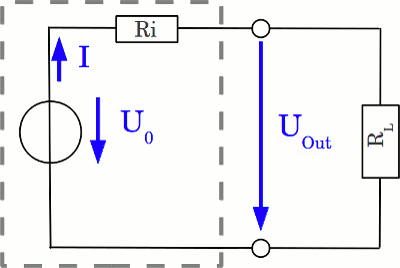
The drawing shows a schematic diagram of a real voltage source, with a load connected to the output clamps. The inner resistance is symbolized by the resistor Ri which is connected in series to the load. The current running through the circuit causes a voltage drop at Ri which is subtracted from the potential U0 generated by the ideal source. At the example above, the inner resistance of the battery can be calculated as follows: The resistance of the filament lamp is: RLamp = 12.3V / 0.8A = 15.4Ω The "resistor inside of the battery" is switched in series to the load and the potential with no load connected is 12.5V, by what we get: RBattery / RLoad = (12.5V - 12.3V) / 12.3V or RBattery = RLoad * 0.2V / 12.3V Resulting in an inner resistance of approximately 0.25Ω. This value is not constant. When connecting a 40W filament lamp to the battery, we get: Potential with no load: 12.5V Potential with 40W filament lamp: 12.0V Current through lamp: 3.8A Resulting resistance of the lamp: 3.2Ω Resulting inner resistance: 1.32Ω Usually there is: The higher the capacitance of a battery, the lower the inner resistance, because the dimensions of the electrodes - mainly the area of their surface - is increasing, too. Voltage regulationThere are some ways to get a more constant voltage than a battery can provide. At the chapter about voltage dividers we have learned how to get a fraction of the voltage provided by a power supply. Let's assume that our circuit needs an input voltage of 5V while the device is connected to the 12V battery from the example above. When using constant resistors, the potential at the output of the voltage divider is decreasing with decreasing voltage of the battery during the discharging procedure or whenever a different load is connected to the circuit. The voltage output of the divider can be readjusted, if one potentiometer is used. The variable resistance of the potentiometer enables you to readjust the output voltage of the divider whenever the battery voltage alters. Another variable resistor is a transistor, which can be used to build a stabilizer circuit: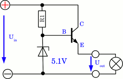
The base pin of the NPN transistor is connected to a voltage divider formed by R1 and the 5.1V Zener diode. Like explained at the chapter about voltage dividers, the zener diode provides an almost constant voltage of 5.1V as long as the input voltage exceeds that value. As soon as a load is connected to the output clamps of the circuit, the emitter-collector line of the transistor and the load are forming the second voltage divider of the circuit. If the resistance of the load is constant, the resulting output voltage across the load is caused by the variable resistance of the transistor's emitter-collector line. Around an emitter-base voltage of 0.5V the resistance is clearly above some Megaohm, while it is decreasing to just some Ohm and below around a base voltage of 0.7V. Usually the resistance of the load is clearly below the maximum and clearly above the minimum resistance of the emitter-collector line, so the emitter-base voltage is always around 0.6V while the circuit is connected to the supply voltage. For the voltage across the load and so the potential at the emitter pin of the transistor there is:
UEmitter = UOut = UIn * RLoad / (RLoad + RTransistor) = UZener - UEB Where is: UEmitter - Potential between ground and Emitter UIn - Input voltage of the circuit RLoad - Resistance of the load RTransistor - Resistance of the transistor's emitter-collector line UZener - Voltage drop across the zener diode (constant) UBE - Emitter-base voltage (nearly constant, approximately 0.6V) What's the message of the formulas above? Well, whenever the resistance of the load is decreasing, the output voltage (which is the voltage across the load) is decreasing, too, resulting in an increasing voltage between Emitter and base (UEB). However with increasing emitter-base voltage, the resistance of the transistor's emitter-collector line is decreasing, resulting in an increasing output voltage. The feedback loop of the circuit counterbalances the falling voltage caused by decreasing resistance of the load. On the other hand: if the resistance of the load is increasing, UBE would decrease causing an increasing resistance of the emitter-collector line. The decrease in resistance of the load is also counterbalanced by a decrease of the resistance of the transistor. An increasing input voltage would result in an increasing output voltage, but also in a decreasing emitter-base voltage and so in an increasing emitter-collector resistance. The increasing resistance of the emitter-collector line counterbalances the increasing input voltage. Vice versa a decreasing input voltage results in an increasing emitter-base voltage and so in a decreasing resistance of the emitter-collector line. Once more the circuit acts contrarious to the varying circumstances, regulating the output voltage to the set point. The resulting output voltage of the circuit is: UOut = UZener - UEB The difference in voltage between input and output voltage must be larger than the base voltage required to bring the bipolar NPN transistor into saturation. That's usually 0.7V (1.3V at Darlington transistors) and above. The minimum required voltage difference from input to output is called dropout voltage. The voltage drop when connecting a load to the output clamps caused by the inner resistance of the voltage source connected to the input clamps has also to be considered, because the output voltage of the regulator circuit can't exceed the input voltage.The switching mode of the transistor is called emitter follower or BJT voltage follower, because the potential at the emitter is following (nearly) that at the base, which is the input of the transistor. The circuit is called linear regulator, because there is a linear correlation between the resistance of the transistor and the input voltage. The resistance of the regulator varies in accordance with the load and the input voltage resulting in a constant output voltage. The transistor is often called pass-transistor, because the device passes the voltage (strictly speaking the current and so the electric energy) from the input to the output circuit. 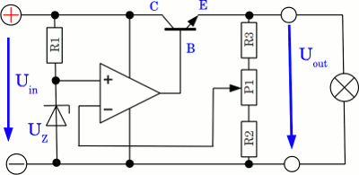
By using an operational amplifier in comparator mode, the stability of the output voltage can be increased significantly: The gain of the operational amplifier is clearly higher than that of a single BJT, hence the transistor is driven with a higher current whenever the voltage at the inverting input drops below that at the non-inverting input, which is connected to the reference voltage at the zener diode. The resulting output voltage can be adjusted to arbitrary value between UZener and (nearly) the input voltage. 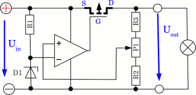
When replacing the NPN transistor by a PNP-type or a p-channel MOSFET, the inverting input has to be connected to the reference voltage, while the non-inverting input has to be connected to the potentiometer. It's a negative feedback loop. The dropout voltage of this regulator type is lower than that at the circuit above, because the pass transistor is driven fully into saturation by attaching a negative voltage between base (gate) and collector (drain). The voltage between emitter and collector (source and drain) which is the minimum dropout voltage, is usually just some millivolts. It's a low drop-out (LDO) regulator. Power dissipationThe linear power supply regulates the output voltage by continually dissipating power in the pass transistor. If the input voltage is 12V, while the output voltage is just 5V and a load of 100Ω is attached to the output clamps, we get for the power dissipated by the transistor:
I = 5V / 100Ω = 50mA Switched regulator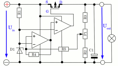
At this circuit, the left operational amplifier is operating as a Schmitt-trigger. The output voltage is not as smooth as at the upper circuit. It is oscillating with an amplitude of approximately 1.0V, depending on the resistance values of R4 and R5. The P-channel MOSFET is turned full-on whenever the input voltage of the Schmitt-trigger reaches the lower threshold and it is turned full-off, when the upper threshold is reached, hence the transistor spends very little time in the high dissipation transitions, so the wasted energy is minimized. Ideally, this circuit dissipates no power, however in a real world there are always losses. The slew rate of the operational amplifier limits the time required to alter the switching state of the transistor (whose slew rate isn't infinite, too) and the switching current always causes some noise which also worsens the efficiency. The second operational amplifier is used to increase the efficiency slightly by reducing the feedback between input and output of the Schmitt-trigger. C1 is required to buffer electric energy at the output circuit. The higher the capacitance, the lower the switching frequency of the transistor. It should be noted that this circuit is only suitable for small currents. I just want to demonstrate a basic principle behind switching regulators!. When the capacitor is charged, a very high current flows, which significantly reduces the efficiency of the circuit. In commercial switching regulators, an inductor is inserted between the MOSFET and positive of the capacitor to limit the high charging current. Dimensions for a circuit suitable for demonstration purposes: Op-amp: LM324N (quadruple device) P-channel MOSFET: IRF9Z34N C1: 1000μF electrolytic capacitor D1: 3.0V Zener diode R1: 1kΩ R2: 12kΩ R3: 12kΩ R4: 1MΩ R5: 12kΩ P1: 100kΩ The lower the value of R5, the closer the thresholds of the Schmitt-trigger and so the smoother the output signal, but the higher the switching frequency and so the losses. 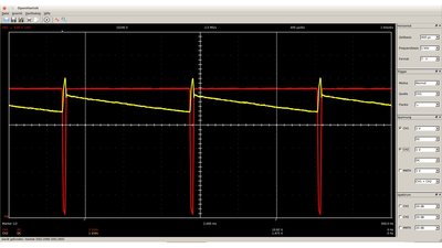
Oscillograph plot of the circuit: Yellow curve: Output voltage Red curve: Base voltage of the MOSFET whenever the output voltage drops below 4.6V, the P-channel MOSFET is turned on. Now C1 is charged until a voltage of 6V is reached and the MOSFET is turned off again. Distortions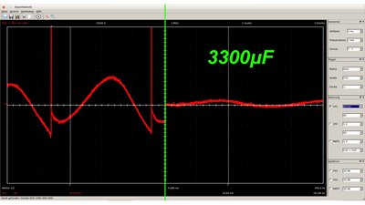
A voltage regulator can't compensate the distortions at the input or output circuit with no lag of time. For example an electric motor connected to the output circuit causes voltage peaks whenever one of it's inductors is turned off abruptly by the commutator. The DC voltage is superposed by an unwanted AC fraction. A simple way of minimizing those distortions is connecting a capacitor in parallel to the output clamps. The higher the capacitance of the device, the better the effect. Electrolytic capacitors are cheap devices with high capacitance and so they are suitable for decoupling unwanted AC components from the DC voltage. The small unwanted residual periodic variation of the direct current output of a power supply is called ripple. Like explained at the chapter about RC-circuits, a low-pass filter can be used to block high frequency AC signals. The higher the resistance or the capacitance of the linear circuit, the better the filter characteristic. ICs often require a very smooth DC voltage while they consume just a low current, so a low-pass filter is a cheap and effective way to eliminate the AC fraction of the input voltage. But remember that the voltage at the power-supply pins of the IC varies with supply current when connected to a low-pass filter (the resistor boosts the inner resistance of the ICs power supply). A typical value for the resistor is 10Ω. 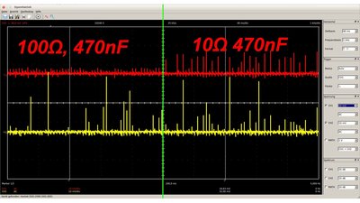
Low-pass filter with 100Ω resistor and 470nF capacitor (left) respectively 10Ω resistor and 470nF capacitor (right). Yellow curve: no filtering Red curve: low-pass filter When replacing the resistor with an inductor of low internal resistance (large diameter of the wound wire), the circuit is also an effective decoupling filter. Small coils of insulated wire, often wound on a magnetic core are commonly used for this purpose as they're very cheap and have no significant series resistance. This type of passive inductor is called choke. The lower the frequency of the AC fraction, the larger the dimensions of the choke, hence they are suitable for filtering very high frequencies. Another advantage of using an LC filter is the efficiency: The electric energy is transformed into heat at the resistor of an RC filter, while it is stored inside of the magnetic field of the inductor when using an LC filter. Considering the small ripple, the total energy dissipated by the resistor is usually negligible. 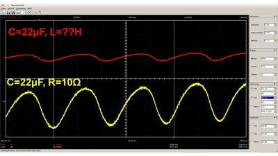
RC versus LC filtering: Yellow curve: RC filter Red curve: LC filter The ohmic resistance of the used inductor is clearly below 10Ω, which is the value of the resistor at the RC filter, however the LC filter is more effective. The frequency of the AC signal is just 330Hz, so a large "choke" was used: It's a toroidal transformer. Constant currentSometimes an application requires a constant current instead of a constant voltage. For example electrolysis is a method of using a direct electric current to drive an otherwise non-spontaneous chemical reaction. Chrome plating is a technique of electroplating a thin layer of chromium onto a metal.As long as the resistance of the load is constant, the current running through the output clamps of a voltage regulator and so through the load is constant, too. If the resistance of the load is decreasing, the voltage is kept on a constant level and so the current is increasing. The regulator circuit has to be altered to get another type of feedback: With decreasing resistance of the load, the voltage output of the circuit must be decreasing, too: 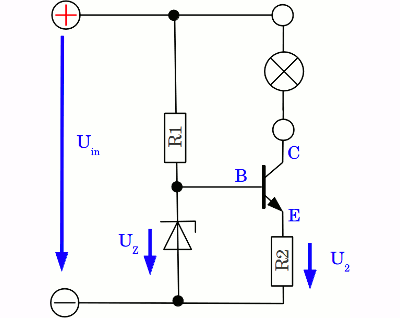
The voltage drop across the zener diode is constant, hence the potential between emitter and base depends on the voltage drop across R2 and so on the current running through the device. For the correlation between emitter-base voltage and the current running through the output circuit and so through the load there is: UEB = UZ - I * R2 Where is:UEB - Emitter-base voltage UZ - Voltage across the zener diode R2 - Resistor I - Current through the output circuit There is a negative feedback loop: If the current running through the output loop and so through R2 is increasing, caused by a decreasing resistance of the load, the emitter-base voltage is decreasing (remember that the zener voltage is constant, while the potential at the emitter is increasing), hence the resistance of the transistor's emitter-collector line is increasing, counterbalancing the decreasing resistance of the load. An increasing input voltage would also cause an increasing current through the load, which is also counterbalanced by an increasing resistance of the transistor. The base voltage is around 0.6V, so for the current running through the output circuit we get: I = (UZ - 0.6V) / R2 When switching a potentiometer in parallel to the zener diode, the current can be adjusted continuously. Keep the maximum power dissipation of the resistor in mind:
PMax = (UZ - 0.6V)2 / R2 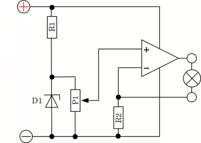
The operational amplifier amplifies the difference in potential between the inverting and the non-inverting input with a high gain, hence the output voltage is increasing until the difference in potential between both input clamps is nearly zero (the voltage at the non-inverting input is constant). There is a negative feedback between input and output circuit: If the resistance of the load is increasing, the current through R2 and so the potential at the inverting input is decreasing, by what the difference in potential between both input clamps is increasing and so the output voltage is increasing, too. With increasing output voltage the current running through the output loop and so the voltage across R2 is increasing. Once again the difference in potential between the input clamps is decreasing to nearly zero and the current is readjusted to the set point. <<< Pulse-width modulation H bridge >>> News The Project Technology RoboSpatium Contribute Subject index Archives Download Responses Games Links Gadgets Contact Imprint |
|
|