|
|
|
|
News The Project Technology RoboSpatium Contribute Subject index Download Responses Games Gadgets Contact <<< Constant voltage Function generator >>> H bridgeThe video about H bridgesBridge circuitA bridge circuit is a type of electrical circuit in which two circuit branches (usually in parallel with each other) are "bridged" by a third branch connected between the first two branches at some intermediate point along them.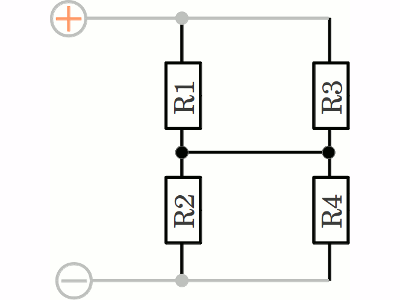
A very simple type of a bridge circuit is called H bridge. You might recognize why it is called H bridge when looking at the drawing. Caused by the bridge, hence the conductive path at the middle of the drawing, the voltage across R2 equals those across R4 and the voltage across R1 equals those at R3 independent from the resistance values of the four resistors. Without the bridge between the two branches, the potential at the mid points depends on the ratio of the resistance values. If 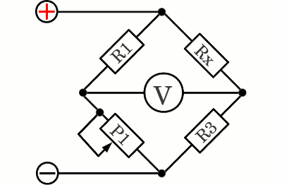
A Wheatstone bridge is used to measure an unknown resistance by balancing the two legs of an H bridge. Two constant resistors (R1 and R3) a potentiometer and the unknown resistor are forming the two legs of a circuit which are bridged by a voltmeter or an ammeter. Like explained, the potential between the two points of the bridge and so the current running across the path is zero whenever the ratio of the resistances of the left leg equals those at the right leg. The potentiometer is varied until the voltage drop between the two mid points is zero when using a voltmeter respectively no current is running through the instrument when using an ammeter. There is a linear correlation between the position of the sliding contact of the potentiometer and the resistance of the unknown resistor, hence the scale of the potentiometer can be calibrated, facilitating the reading of the resistance value of the unknown resistor. Forward / reverse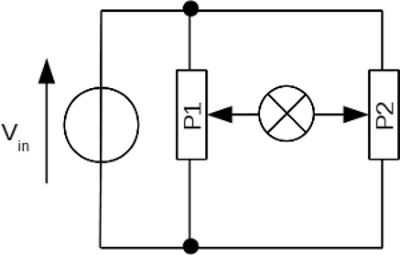
At the chapter about voltage dividers, an H bridge consisting of two potentiometers was introduced, enabling you to apply any voltage between +VIn and -VIn to a load connected between the two potentiometers. While potentiometers are suitable to adjust the voltage of low power devices manually, transistors can be used to control even high power devices by nearly any electronic circuit: 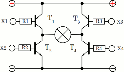
This H bridge is composed of two NPN and two PNP transistors. The resistance of the lower, NPN transistors is decreasing while the potential between ground (=negative terminal) and X2 respectively X4 is increasing. The resistance is minimal, if the potential at the input clamps equals the input voltage of the circuit. The series resistors connected to the base pins are limiting the base current. In contrast, the resistance of the PNP transistors is minimal when the potential between ground and X1 respectively X3 is zero volts while it is maximal, if the potential at the input clamps equals the input voltage. T2 and T4 are called low side transistors, while T1 and T3 are called high side transistors. 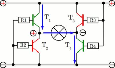
When connecting X1 and X2 to ground respectively X3 and X4 to the positive supply voltage, the resistance of T2 and T3 is at it's maximum (above some Megohm), while those of T1 and T4 is at it's minimum (below some Ohm). As a result, the potential at the mid point of the left leg of the circuit equals (almost) the supply voltage, while those at the mid point of the right leg is (nearly) zero. A current is running from the positive terminal via T1 from the left to the right through the load and finally through T4 to the negative terminal of the voltage source. The positive terminal is at the left side of the load. 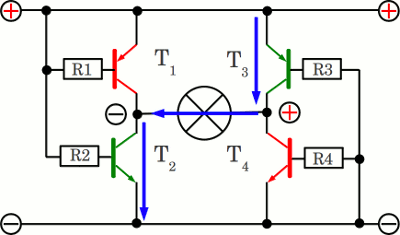
The situation alters, if X1 and X2 are connected to the positive supply voltage while X3 and X4 are connected to ground. Now the positive terminal is at the right side of the load and the current is running through T3 respectively T2. 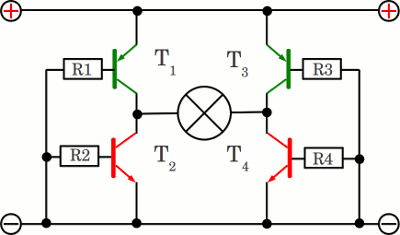
When connecting all four input clamps to ground, the upper PNP transistors are turned "on", while the lower NPN transistors are turned "off". The potential at both clamps of the load equals nearly the positive supply voltage, hence there is no current running through the load. 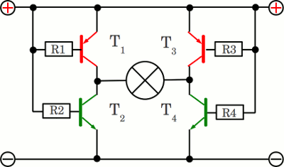
When connecting all four input clamps to the positive terminal of the supply voltage, the upper PNP transistors are turned "off", while the lower NPN transistors are turned "on". The potential at both clamps of the load equals nearly the negative supply voltage, hence there is also no current running through the load. 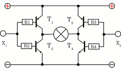
Usually there are just two input clamps:
Step up / down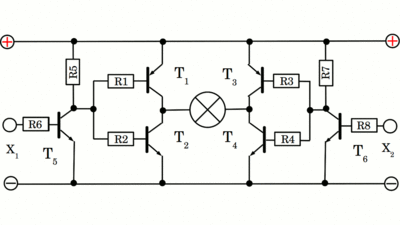
If the operating voltage of the H bridge differs from the HIGH level at the inputs (e.g. the motor needs 12V while the computer used to control the bridge has a logic HIGH level of just 3.3V), a step up transistor (T5 and T6 in the drawing) is needed at each of the inputs (see Voltage level conversion section below). Half bridge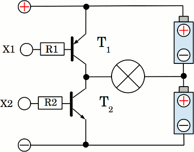
An H-bridge composed of four transistors is named full bridge. With a split supply, a half bridge is sufficient to control a load with alternating current. Two batteries are used in the illustration shown here. 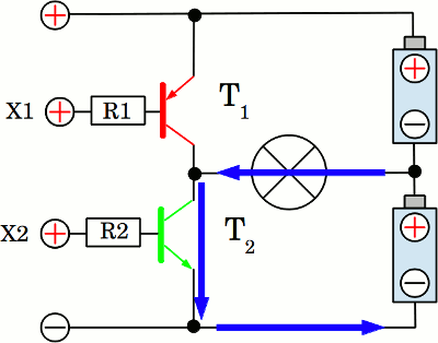
If the base pins of both transistors are connected to the positive terminal through the series resistors, hence there is a HIGH signal at the inputs, the upper PNP type is turned "off", while the lower NPN type is turned "on". A current exits the positive terminal of the lower battery, running from the right to the left through the load and via transistor 2 it reenters the battery at the negative terminal. 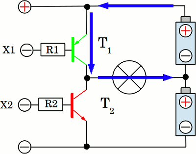
If both inputs of the half bridge are connected to the negative terminal, the upper PNP type is turned "on" and the lower NPN type is turned "off". The current runs from the positive terminal of the upper battery trough transistor 1, now from the left to the right through the load and back to the negative terminal of the battery. An advantage of using half bridges is the lower number of needed transistors, a disadvantage is the more complex power supply. MOSFETsWhen composing an H bridge of bipolar junction transistors, the base current required to bring the transistors into saturation mode has to be considered. The dimension of R1 - R4 depends on the supply voltage. The resistance value has to be doubled when operating the circuit with an input voltage of 12V instead of 6V. The power dissipated by the resistors is also doubled if the resistance values are adapted to the higher voltage and it is quadrupled if not. So the maximum power dissipation has also to be kept in mind.Using n-channel respectively p-channel MOSFETs instead of NPN or PNP types gives you some benefits: 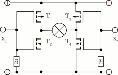
Just two pullup or pulldown resistors are required and the value of R1 respectively R2 is not critical, simply use a relative high value to avoid operating near the maximal power dissipation. The minimal input voltage of the circuit is affected by the source gate voltage required to turn the MOSFETs reliably "on" (it must be slightly higher than the threshold voltage VGS(th)). The maximal input voltage should be clearly below the maximal source gate voltage to avoid operating at the limit. Keep voltage peaks in mind when switching inductive loads. 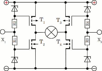
If the supply voltage exceeds the maximal source gate voltage of the MOSFETs, four voltage dividers, each composed of a zener diode and a constant resistor should be inserted. The zener voltage must be greater than the threshold voltage required to turn the transistors "on". Now the maximal source drain voltage, which is usually significantly higher than the maximal source gate voltage, limits the input voltage of the circuit. 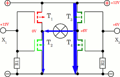
The clamps must always be connected to either the positive or the negative supply voltage. If X1 is connected to the positive supply voltage, while there is just half the supply voltage (+6V) attached to X2 the potential between T1 and T2 is nearly 0V, those between T3 and T4 is approximately 6V, because the resistance of T3 equals those of T4. In sum there is a potential of 6V from the left to the right across the load. But keep in mind that the resistance of T3 and T4 is relatively low, hence a high current is running through the right leg of the circuit! During a switching operation of the H bridge, meaning whenever the potential at one of the clamps alters from the positive supply voltage to zero or vice versa, there is always a high current running through the legs of the circuit for a short span of time. The overlapping turn on time is called cross conduction or shoot-through. 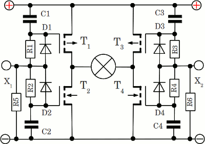
A turn-on delay, implemented by a linear RC circuit, prevents the shoot-trough. Whenever the voltage at X1 alters from the positive supply voltage to zero volts, C1 gets charged slowly via R1, hence the turn on procedure of T1 is delayed. In contrast C2 gets discharged quickly through D2 which is forward biased, hence T2 is turned off with almost no delay. R5 and R6 are pulldown resistors. 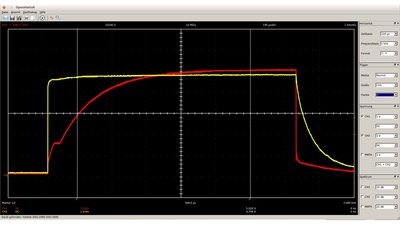
Two linear RC circuits, each composed of a 47kΩ resistor and a 1nF capacitor delays the turn on procedure of the MOSFETs. The high side MOSFET (yellow curve) is turned off immediately, because the discharging current of C1 is running through the forward biased diode (D1). The turn on procedure of the low side MOSFET is delayed, because the charging current of C2 is running through R2. At the falling edge of the signal, the turn off procedure of the low side MOSFET (red curve) is faster than the turn on procedure of the high side MOSFET, because now D2 is forward biased. PWMIf partial power is required for the load, the H-bridge can be controlled by pulse-width modulation. To avoid the cross conduction during each switching operation of the pulse-width signal, the circuit has to be altered: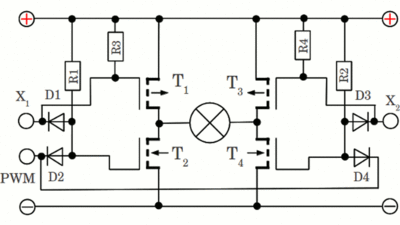
The p-channel MOSFETs are still switched directly by the signal at X1 respectively X2, while the n-channel MOSFETs are controlled by the signal at X1 AND the pulse-width signal respectively X2 AND the pulse-width signal. If the positive supply voltage is attached to X1, T1 is turned "off". T2 is not turned "on" until the pulse-width signal is also on "high" level. If one of the clamps is connected to ground, T2 is turned "off", because D1 or D2 or both are forward biased, pulling the gate of T2 to ground. On the other hand if X1 is on "low" level, T1 is always turned "on", while T2 is alway "off" even if the pulse-width signal is at high level, because, the potential at the base of T2 is always pulled to ground via D1. The same is for X2 and the pulse-width signal. With X1 and X2, the polarity of the voltage across the load can be controlled, while the power control is done via the pulse-width signal at the third input clamp. The diodes are forming an AND gate. Whenever the polarity is altered, a shoot-through will occur if the pulse-width signal is at high level. Ensure that the PWM signal is set to "low" level before altering the polarity. Voltage level conversionWhen operating the H bridge at an input voltage of 12V , the "high" level at the input clamps must also be 12V. For example computers provide an output voltage of just 5V or 3.3V. The solution of the problem is to insert three amplifying circuits: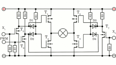
By using MOSFETs, the current running through the input clamps is minimized to the fraction running through the pulldown resistors R6 - R8. Keep in mind, that the voltage level gets inverted by the amplifying stages: For example a "high" level at the input clamp of the pulse-width signal becomes a "low" level at D2 and D4, hence a "low" level at the pulse-width signal is required to power the load between the midpoints of the H bridge. Vice versa, a "high" level at the pulse-width signal is required to prevent cross conduction when altering the polarity of the H bridge. Flyback diodesLike mentioned at the chapter about pulse-width modulation, a flyback diode can be used to minimize distortions caused by inductive loads. Those diode has to be connected in parallel to the load, but with reverse polarity. When using an H bridge to control a load, the polarity can be altered, hence the diode would become forward biased! To avoid this, 4 diodes are required to create the wanted effect of a single flyback diode at a single switch: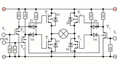
If the positive potential of the induced voltage is at the left side of the load, a current running through D5 and D8 is eliminating the voltage spike. Vice versa, if the positive potential is at the right side and so the negative potential at the left, the current is running through D6 and D7. The maximal current of the diodes should not be lower than the maximal drain current of the MOSFETs. The voltage drop across forward biased Schottky diodes is lower (0.15-0.45 volts) than those of silicon types (0.6-1.7 volts), so the power dissipated by the devices is clearly lower. The following devices were used for the H bridge demonstrated at the video: T1, T3 = P-channel MOSFET IRF9Z34N T2, T4 = N-channel MOSFET IRLZ24N T5 - T7 = N-channel MOSFET 2N7000 R1 - R8 = 12kΩ D1 - D4 = low power silicon diodes D5 - D8 = Schottky diodes e.g. SB2040 The circuit can be operated with a supply voltage of 5-12V. The voltage level at the input clamps should be above 3V. The current through the load should be below 5A when operating the transistors without a heat sink. Simple control
When removing the pull-down resistor at X2 and connecting those input clamp to the drain pin of T5, which is the MOSFET used to amplify the signal of X1, two input pins are sufficient to control the H bridge. X1 controls the polarity of the H bridge: The positive pole is at the left side of the load while X1 is connected to "high" level and the positive pole is at the right side, while X1 is connected to "low" level. The second pin is the pulse-width signal, used to control the power supplied to the load. The less input clamps at the H bridge, the less output clamps at the computer or microcontroller are required to control the device. The disadvantage is a lower felxibility. To activate the braking functionality discussed below, at least three input clamps are required (X1, X2 and PWM). Dynamic brakingWhen switching the motor of an electric vehicle by an H bridge, another effect of the flyback diodes has to be considered: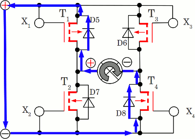
Caused by the inertia, the vehicle won't stop immediately if no more power is delivered to the motor. The motor continues spinning and starts operating as a generator. The polarity of the thereby induced voltage is identical to those applied to the motor beforehand. The current running through the flyback diodes and through the windings of the motor is now slowing down the vehicle, remember that mechanical energy is converted into electric energy. Those procedure is called dynamic braking. A fraction of the generated electric power is dissipated as heat in the flyback diodes and the wire of the motor, while the rest is returned to the supply line. A more complex circuit is required to return the generated power safely to the battery of the vehicle, which is called regenerative braking. 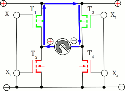
Without the flyback diodes, the dynamic braking can be controlled by the H bridge: If all transistors are turned "off", no current is running through the windings of the motor, hence the wheels are spinning without being slowed down by dynamic braking. Of course, the peaks of the induced voltage have to be considered. To activate the process of dynamic braking, the two low side or the two high side MOSFETs have to be turned "on". Now there is a conductive path between the clamps of the motor and the vehicle is actively slowed down while electric power is generated. The electric power is dissipated as heat in the transistors and the wire of the motor, which is why those kind of braking is called rheostatic. N-channel MOSFETs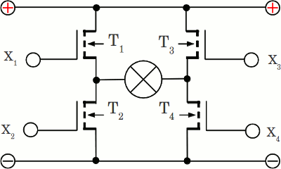
The majority charge carriers of p-channel MOSFETs are holes, whose mobility is lower than those of electrons, the majority charge carriers inside of n-channel types. As a result, the on-resistance of p-channel MOSFETs is usually higher than those of n-channel MOSFETs, assuming identical dimensions of the devices. To minimize the power dissipated by an H bridge, four n-channel MOSFETs can be used instead of two n-channel types at the low side and two p-channel types at the high side. 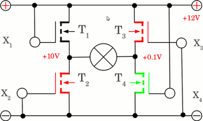
Let's assume, the circuit is connected to a power supply with an output of +12V. X3 is connected to ground, hence T3 is turned "off". X4 is connected to +12V, hence T4 is turned "on". The potential at the right mid point is nearly 0V. The situation is tricky at the left half bridge: X2 is connected to ground, hence T2 is turned "off". X1 is connected to +12V, so what's the potential between source and gate of T1? If T1 would be turned "on", the potential at the mid point of the left half bridge was approximately 12V. So the difference between source and gate of T1 was nearly 0V, turning T1 "off". If T1 and T2 are both turned "off", the potential at the mid point would be around +6V, causing a source gate voltage of 6V at T1 which is sufficient to turn those device "on". So the truth is between the two extremal values. If the threshold voltage of the n-channel MOSFET is around 2V, the system will tend to a potential of approximately 10V at the mid point with T1 turned partly "on". 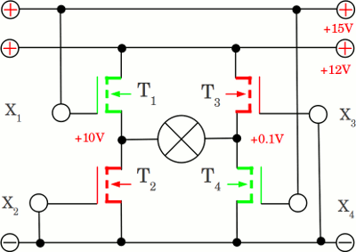
To be able to turn T1 fully "on", a potential above 14V (12V + 2V threshold) at the gate pin of the high side MOSFET and so a second power supply is required. The circuit driving the MOSFETs is more complex than those of an H bridge composed of p-channel MOSFETs at the high side. <<< Constant voltage Function generator >>> News The Project Technology RoboSpatium Contribute Subject index Archives Download Responses Games Links Gadgets Contact Imprint |
|
|