|
|
|
|
News The Project Technology RoboSpatium Contribute Subject index Download Responses Games Gadgets Contact <<< Switch Voltage divider >>> Operational amplifiersThe video about op-ampsIntegrated circuitsLike explained at the chapter about amplifying circuits, it is tricky to build circuits with a high gain. Many factors like temperature drift, crossover distortions or linearity have to be considered to minimize the distortions caused by the electronic circuits. Several components are required to build one ore more pre-amplifier(s) and a power circuit. Today, it is more easy to integrate a large number of transistors, capacitors or resistors into a small chip instead of assembling a circuit manually by using discrete electronic components. Amplifying circuits with different properties are available as cheap and tiny chips. A special group of amplifying circuits is called operational amplifiers or short op-amp. The drawing below, which is from Wikipedia, shows a component level diagram of the common 741 op-amp.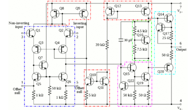
You would need a large board to build this circuit by using discrete components... Functionality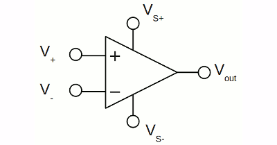
The drawing shows the circuit diagram symbol for an operational amplifier. The functionality of the pins is: VS+ - positive power supply VS- - negative power supply V+ - non-inverting input V- - inverting input Vout - output An op-amp amplifies the voltage drop between V+ and V-, which is called the differential input voltage. Operational amplifiers are often used with a symmetrical bipolar power supply, hence the referential potential (ground) is half the total voltage between the negative and the positive supply voltage. While the difference in potential at the two input clamps is zero (e. g. they are shortened), the resulting output voltage of an ideal operational amplifier is also zero volts which is sometimes called virtual ground meaning the output clamp of the op-amp is at a steady reference potential, without being connected directly to the reference potential. Real devices normaly require a differencial DC voltage between the input clamps to make the output zero volts. This parameter is called input offset voltage (Vos) and it is usually around 0.1mV. 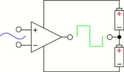
The gain of integrated circuit op-amps is typically 100000 or more, so a voltage drop of just +0.1V between the two input clamps would result in an output voltage of +10000V. Like mentioned at the chapter about amplifying circuits, the voltage drop at the output can't exceed the value of the supply voltage, so the output signal gets clipped. Situations in which the output voltage is equal or greater than the supply voltage are referred to as saturation of the amplifier. A sine curve with a peak voltage of just 1mV between the input clamps becomes a square wave signal at the output clamp. Negative feedback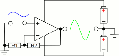
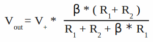
If your intention is to amplify a sine wave signal, an op-amp with a gain of more than 100000 is nearly useless. By applying a portion of the output voltage to the inverting input, the total gain of the circuit can be reduced. At the drawing, the signal source is attached between ground and non-inverting input of the op-amp. R1 and R2 are forming a voltage divider between output of the op-amp and ground. The inverting input is attached between R1 and R2. Let's assume the following values: The gain of the op-amp is 100000, R1 = 1kΩ, R2 = 10kΩ. VS- is attached to -12V, VS+ to +12V. The situation is simple when attaching 0V to the non-inverting input: The output voltage is 0V and the resulting voltage drop at R1 and so the inverting input is 0V. What's happening if the input voltage at the non-inverting input jumps up to 0.1V? The resulting differential input voltage is now 0.1V, the gain is 100000, hence the voltage output would climb up to 10000V, but it is clipped at +12V. Now that 12V are attached to the voltage divider, the resulting voltage drop at R1 is (1) Vout = (V+ - V-) * β and (2) V- = Vout * R1 / (R1 + R2) By inserting equation (2) in (1) we get: Vout = (V+ - (Vout * R1 / (R1 + R2))) * β Solving the equation for Vout:
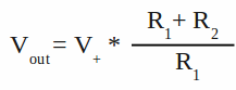
Where is: V+ - Voltage drop between non-inverting input and ground (=input voltage) V- - Voltage drop R1 Vout - Voltage output op-amp R1, R2 - Resistors of the voltage divider β - Voltage gain of op-amp For very high values of β, the equation can be simplified to:
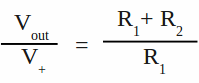
The voltage gain Vout / V+ of the op-amp with negative feedback is: Adding a negative feedback via a voltage divider reduces the gain of an op-amp. The overall gain Vout / V+ is called closed-loop gain (ACL), because of the feedback provided by the resistors of the voltage divider. Without a feedback loop, the overall gain of the op-amp is called open-loop gain (AOL) Comparator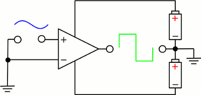
Without negative feedback, an op-amp acts like a comparator. At the drawing, the inverting input is connected to ground, hence the output will be maximum positive if the voltage applied to the non-inverting input is positive. If the input voltage becomes negative, the output will be maximum negative. The output of the op-amp can be either VS- or VS+ so it indicates if the input voltage is larger or lower than 0V. 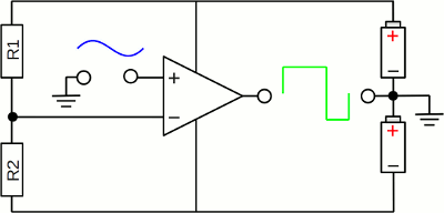
By connecting the inverting input to a voltage divider, the voltage of the non-inverting input can be "compared" to any voltage level between VS- and VS+. When connecting the non-inverting input to the voltage divider, the output signal is VS+ if the voltage at the inverting input is lower than that at the non-inverting input, respectively it becomes VS- if it climbs above that value. Now, the output signal is inverted. Schmitt trigger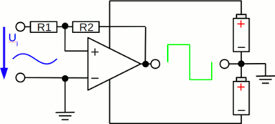
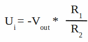
Besides the negative feedback described above, we can also apply a positive feedback to an op-amp. Let's have a closer look at the behaviour of the feedback network of the drawing, assuming a resistance of 1kΩ for R1, 10kΩ for R2, a positive supply voltage of +12V and a negative supply voltage of -12V: While connecting the circuit to a voltage source, Ui and V- and so the output voltage are zero, but just a slight random variation of V+ causes the output voltage to tilt either to the maximum or minimum value. Let's assume the output voltage is at it's maximum value and the input voltage is +0.1V. With the feedback via the voltage divider we get: (3) V+ = Ui + (Vout - Ui) * R1 / (R1 + R2) = 1.18V When the input voltage is decreasing to 0V we get (remember the output voltage is still +12V): V+ = 0V + (12V - 0V) * 1000Ω / (1000Ω + 10000Ω) = 1.09V Even at an input voltage of -0.1V we get: V+ = -0.1V + (12V + 0.1V) * 1000Ω / (1000Ω + 10000Ω) = 1.00V The op-amp will tilt to the minimum supply voltage, as soon as V+ drops slightly below 0V. Inserting V+ = 0 and solving equation (3) to Ui gives us: Where is: Ui - Input voltage of the circuit Vout - Voltage output of the op-amp R1, R2 - Resistors of the voltage divider To cause the op-amp to switch from +12V to -12V, the input voltage of the circuit must drop slightly below -1.2V. Now that the output voltage is -12V, let's increase the input voltage to 0V: V+ = 0V + (-12V - 0V) * 1000Ω / (1000Ω + 10000Ω) = -1.09V The voltage output of the op-amp at an input level of 0V is now -12V! The input voltage of the circuit must rise above -(-12V) * R1 / R2 = +1.2V to cause the op-amp to switch back to an output voltage of +12V. 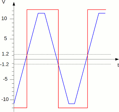
Input (blue) and corresponding output (red) signal of a Schmitt trigger: On a normal comparator, the op-amp will switch at the same point of the rising and falling edge of the input signal. The output signal of the op-amp will start oscillating while the input signal is near the threshold, whenever the input voltage crosses the threshold because of noise. On a Schmitt trigger, the situation is different: The output signal is low, while the input signal is below a certain threshold and it is high if it is above a different (higher) threshold. The output signal retains it's value while the signal is between the two different input levels. 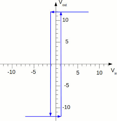
The dual threshold action is called hysteresis. The output voltage of the Schmitt trigger depends not only on the current input voltage, but also on that in the past. For example the output voltage at an input signal of 0.1V can be either +12V or -12V. It is +12V if the input signal was above +1.2V and is now falling to +0.1V. Vice versa the output signal is -12V if the input signal was below -1.2V in the past and is now rising to 0.1V. Single supply voltage Schmitt-Trigger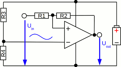
This diagram shows a Schmitt trigger with a single supply voltage. Half the supply voltage is attached to the inverting input using a voltage divider composed of two identic resistors (R3 and R4). Twilight switch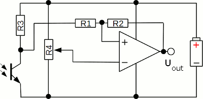
Just one practical circuit with a single supply Schmitt trigger: The input voltage is provided by a voltage divider with one constant resistor (R3) and one PNP-phototransistor. If the phototransitor is exposed to light, the resistance decreases, hence the input voltage is decreasing, too. If the lower threshold is reached, the output voltage of the Schmitt-trigger drops down to 0V, hence a device (maybe a lamp) connected to the output clamp is turned off while the sun is shining. R4 is a potentiometer, operating as a voltage divider at the inverting input of the op-amp, by what the threshold can be adjusted, so that the light is switched off during twilight rather than in bright sunlight. Ideal op-amp versus LM324N
<<< Switch Voltage divider >>> News The Project Technology RoboSpatium Contribute Subject index Archives Download Responses Games Links Gadgets Contact Imprint |
|
|