|
|
|
|
News The Project Technology RoboSpatium Contribute Subject index Download Responses Games Gadgets Contact <<< RC circuit Pulse-width modulation >>> Flip-flop / multivibratorThe video about multivibratorsFlip-flop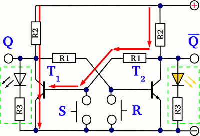
At one of the previous chapters we have learned how to use a transistor as an electronic switch. At this chapter we will see how a transistor can be used to switch another one. At the drawing you can see a pair of cross coupled transistors. S (set) and R (reset) are the input push buttons of the circuit, while Q and Q are the output clamps. While using a transistor as a switch, the state of the device can be either "on" (the voltage drop at the emitter-collector line is nearly zero) or "off" (the voltage drop at the emitter- collector line equals nearly the supply voltage of the circuit). So what happens, if the left transistor (T1) is turned "on"? The base pin of T2 is connected via a series resistor to the collector pin of T1, so if the voltage drop at the emitter-collector line of T1 is (nearly) zero, the voltage drop at the base pin of T2 and so the current running through those pin is also zero, hence T2 is turned "off". While the voltage drop at the emitter-collector line of T2 equals (nearly) the supply voltage, the voltage feedback passed to the base pin of T1 and so the current running through the base of T1 is at it's maximum, causing T1 to be turned "on". So the state of the circuit is stable: While T1 is turned "on", T2 gets turned "off", providing a feedback voltage which sustains the switching state of T1 ("on"). The voltage drop at Q is zero, while those at Q equals the supply voltage. The LED - which is optional - at Q is turned on, while those at Q is turned off. 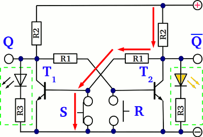
What is happening while pushing button S? The current running through the base pin of T1 prior to this is now cut off, because the emitter base line of the transistor is shortened. Consequently T1 is turned "off", which is why the voltage drop at the emitter collector line increases to nearly the supply voltage. 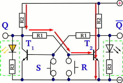
The voltage feedback passed to the base pin of T2 causes the right transistor to alter it's state from "off" to "on". Now that T2 is turned "on", the feedback passed back to the base of T1 is zero. 
Even if the switch S is released, the circuit retains the switching state. Now the voltage drop at Q is nearly the supply voltage, while those at Q is nearly zero. The LED at Q is turned on, those at Q is turned off. Pushing button S once again doesn't alter the state of the whole circuit, because the base pin of T1 is already shortened by the emitter-collector line of T2. 
While T2 is turned "on" and button R is pushed, the base pin of T2 gets shortened, altering the switching state of those transistor from "on" to "off" which in turn alters the switching state of T1 from "off" to "on". By pushing the S button, the output Q of the circuit is set, while it is reset by pushing the R button. Q is the inverting output of the circuit: Whenever Q is set (the voltage output equals the supply voltage), Q is reset (the voltage output is zero) and vice versa. The circuit is called flip-flop, latch or bistable multivibrator. 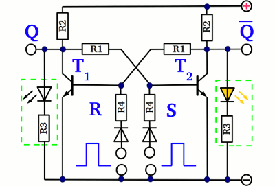
If your intention is to operate the flip-flop by electric pulses instead of mechanical switches, two resistors (R4 = R2) and two diodes have to be inserted. Now the transistors are turned "on" by a positive voltage. Because of the diodes, the transistors are not turned "off" if the input voltage drops to zero. For a demonstration circuit you can use: T1, T2 = BD175 R1 = 100kΩ R2 = 560Ω R3 = 1kΩ R4 = 100kΩ Monostable multivibrator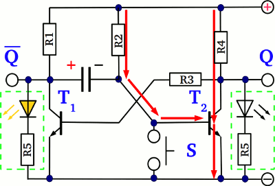
In comparison to the flip-flop drawn above, the circuit is now altered slightly: The coupling resistor at the base of T2 has been replaced by a capacitor and an additional resistor is connected between the terminal of the supply voltage and the base pin of T2 (here denoted as R2). At the initial state, T2 is turned "on", pulling the base voltage of T1 to ground via the coupling resistor R3, hence T1 is turned "off". The base current of T2 is running from the positive terminal via R2, retaining the switching state of the circuit. What about the voltage across the capacitor at this stable state of the circuit? The left side of the capacitor is connected to the collector pin of T1, which is turned "off", hence the potential at those pin equals nearly the supply voltage VS. The right side of the capacitor is connected to the base pin of T2 which is turned "on", hence a potential of approximately 0.7V is applied to those pin (see properties of BJTs for details). The resulting voltage drop is 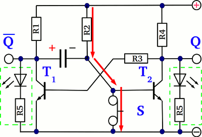
If the button S is pushed, the emitter-base line of T2 gets shortened... 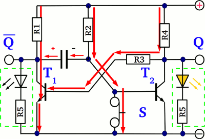
...and T2 is turned "off". Via the coupling resistor R3, T1 is turned "on". So what about the voltage drop across the capacitor at this state? The left side is pulled to (nearly) ground via T1 (which is conductive) and the right side is pulled to ground via the push button (which is conductive, too). The resulting voltage drop is (nearly) zero. The voltage across the emitter-collector line of T1 depends on the electrical properties of the used BJT, let's say it's 0.1V. It must be clearly lower than 0.7V or else T2 is never turned off by T1. A discharging current is running through the capacitor for a short span of time until the voltage across the capacitor drops from the initial value 
If the button S is released, the right side of the capacitor is no longer pulled to ground level by the switch, hence the device gets charged via R2 with reverse polarity (compared to the initial state). The initial voltage across the capacitor during the charging procedure depends on the time span, the button was pushed. Like explained above, there is an disequilibrium of charge across the capacitor when T1 switches from "off" to "on". If the button is pressed long enough, so that those disequilibrium can be balanced by a current running through the switch and the emitter-collector line of T1, the charging procedure starts with an initial voltage of approximately -0.1V. If the button is pushed for a very short span of time, so that there is still a voltage of approximately The turn off time of T2 depends on the time, the button is pushed! 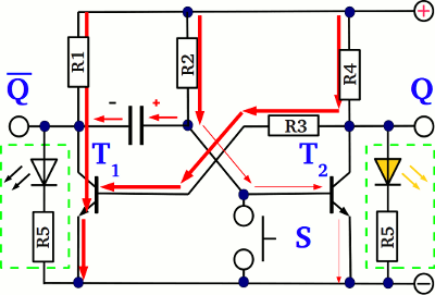
During the (reverse) charging procedure, the polarity of the capacitor alters. The left side of the capacitor is still pulled to (nearly) ground level via T1... 
...so the circuit can be simplified by this one: While the capacitor gets charged (see chapter RC circuits for details) via R2, the voltage at the base of T2 is increasing. 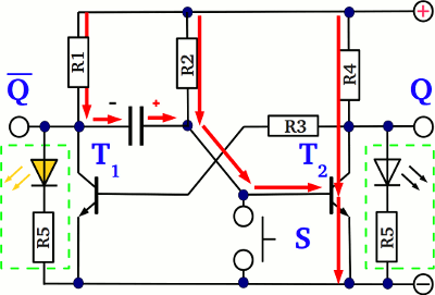
If the potential across the capacitor exceeds a voltage of 0.6V, the resistance of the emitter-collector line at T2 is decreasing clearly - the transistor is turned "on" again. Via the coupling resistor R3, T1 is turned "off", by what the potential at the left plate of the capacitor is increasing from zero volts to nearly the supply voltage, while the voltage drop across those device is still around 0.7V. The potential equalization takes place via the resistor R1 at the left plate and via the base of T2 on the right plate. Both devices are relatively high resistive, hence the potential at the collector pin of T1 is increasing slowly and an additional current is running through the base of T2 for those span of time. There is a positive feedback loop: With increasing base current the resistance of T2 is decreasing, causing an increasing resistance of T1 via the coupling resistor R3, which in turn lifts the left plate of the capacitor to a higher potential and so provides a higher base current through T2 driven by the disequilibrium of charge cumulated inside of the capacitor. 
The capacitor gets discharged respectively charged with the initial polarity via R1 and the base pin of T2. The polarity of the capacitor alters during the charging procedure and finally the initial state of the circuit is reached. The slew rate of the rising edge at Q is lower than those at the falling edge at Q with no capacitor attached to the collector of T2 (see explanation astable multivibrator below). 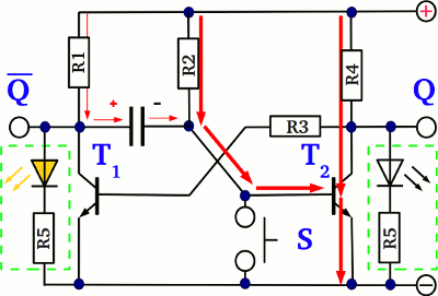
The whole process in animation. The maximum voltage across the capacitor from the right to the left plate is +VS. The minimum voltage is -0.7V. So if you are using an electrolytic capacitor, the negative terminal must be connected to the base of T2 and the positive terminal to the collector of T1. The lower the resistance of R1, the lower the output impedance and the higher the slew rate at the rising edge of Q, but the higher the current running through the device while T1 is turned "on". The minimum resistance of R1 depends on the supply voltage of the circuit and the maximum power dissipation: Rmin = U2 / Pmax Where is:Rmin - minimum resistance of R1 U - supply voltage of the circuit Pmax - maximum power dissipation of R1 The same resistance value should be used for R4. The turn on time of T1 is limited by the resistance of R2 and the capacitance of the RC network. For more information read the paragraph about the astable multivibrator below. The maximum resistance of R2 depends on the characteristics of T2. The maximum base current of T2 is limited by those device. The base current must be high enough, so that the voltage drop at the emitter-collector line is clearly below 0.7V (at least 0.1V) while the maximum base current is running. R3 equals R2. T1 and T2 must be NPN types. 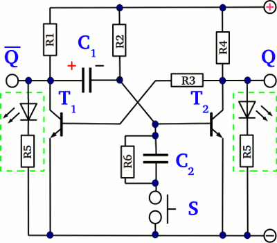
The circuit can be altered with another capacitor respectively resistor to get just a small pulse, while actuating the push button: By pushing the button, C2 is switched in parallel to the base of T2, hence the voltage drops to zero, because the capacitor was discharged beforehand. As long as the button is pushed, C2 gets charged via R2. The lower the capacitance of C2 (it must be clearly lower than those of C1), the faster the charging procedure and so the higher the voltage across C2 after a very short span of time, resulting in a short turn-off time of T2. When the button is released, C2 gets discharged via R6, whose resistance should be clearly higher than those of R2. So the initial state is reached. For a demonstration circuit you can use: T1, T2 = BD175 R1, R4 = 560Ω R2, R3 = 100kΩ R5 = 1kΩ R6 = 100kΩ C1 = 22μF C2 = 1nF 
Curve progression at the base pin of T2, which is identical to those at C2 while the button is pressed. As soon as the push button is closed, the voltage drops below 0.6V (C2 was discharged beforehand), which is why T2 is turned "off". T1 gets turned "on" via R3, hence the voltage at the base of T2 and so at the upper plate of C1 is decreasing to -9.4V during 40μs. Now the turn on time of T1 respectively the turn off time of T2 is running until C1 gets charged from -9.4V to +0.6V via R2. Astable multivibrator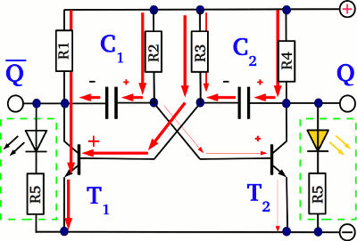
When replacing the coupling resistor R3 of the monostable multivibrator by a second capacitor-resistor network, the resulting circuit is an astable multivibrator. Let's discover the functionality while T1 is turned "on" and T2 is turned "off". The voltage across C1 is lower than 0.6V, which is why the base current running through T2 is very low, hence the resistance of the emitter-collector line is very high. The left plate of C2 is connected to the base pin of T1 which is turned "on", hence the potential is approximately 0.7V. The right plate of the capacitor is connected to the collector of T2, which is turned "off", hence the potential is around the supply voltage (VS). The total voltage across C2 from the left to the right plate is: The left plate of C1 is connected to the collector of T1 which is turned "on", hence the potential in relation to the negative terminal is around 0.1V (the exact value depends on the base current and the electrical properties of the used BJT). It is important, that the voltage drop across T1 is clearly lower than 0.7V or else T2 can not be turned "off" by T1. The potential at the right plate and so the voltage across C1 is increasing, because the device is connected to the positive supply voltage via R2. 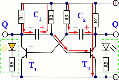
While the voltage across C1 is increasing, the base current through T2 is increasing, too. Around a base voltage of 0.6V, the resistance of the emitter-collector line is decreasing clearly, hence the potential at the right plate of C2 drops from nearly the positive supply voltage to approximately 0.1V, while the voltage drop across the capacitor from the left to the right plate is still 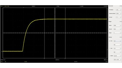
The slew rate at the rising edge at Q is lower the higher the capacitance of C1 respectively the resistance of R1, because the voltage across C1 acts contrarious to the polarity of the voltage source. 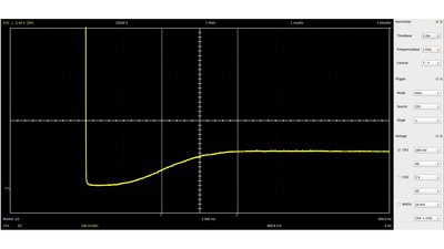
In contrast the voltage drop across C2 boosts the difference in potential caused by the voltage source, hence the slew rate at the falling edge at Q is very high. The disequilibrium in potential caused by the right plate of C2 is balanced by a current running through the emitter-collector line of T2 which has a low resistance, so there is a slight distortion at the end of the falling edge. 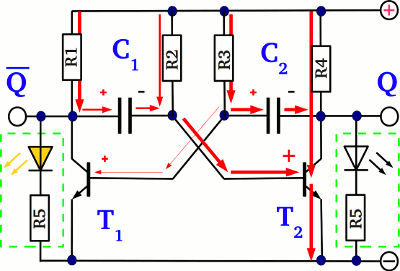
Now the situation is similar to those at the start of the procedure apart from the fact that T1 is turned "off" while T2 is turned "on". A charge current is running through R3 and C2 until the circuit alters its state at Q / Q once again, reaching the initial state. 
The whole process in animation. The turn on/off time for the astable multivibrator is given by the resistance respectively the capacitance of the coupling rc-network: [9.4] T = ln(2)RC Where is:T - turn on / off time (=period) R - resistance value of R2 respectively R3 C - capacitance of C1 respectively C2 Note the dimensions of the devices like explained above (monostable multivibrator): The maximum voltage across the capacitors is +VS. The minimum voltage is -0.7V. So if you are using an electrolytic capacitor, the negative terminal must be connected to the base of T1 respectively T2 and the positive terminal to the collector of T2 respectively T1. The lower the resistance of R1 respectively R4, the lower the output impedance and the higher the slew rate at the rising edge of the signal at Q respectively Q, but the higher the current running through the devices while T1 respectively T2 is turned "on". The minimum resistance of R1 respectively R4 depends on the supply voltage of the circuit and the maximum power dissipation (see above). The maximum resistance of R2 respectively R3 depends on the characteristics of the used transistors. The maximum base current is limited by those devices. The base current must be high enough, so that the voltage drop at the emitter-collector line is clearly below 0.7V (at least 0.1V) while the maximum base current is running. T1 and T2 must be NPN types. Suitable values are: R1, R4 = 560Ω T1, T2 = BD175 For a visible blinking frequency of 0.66Hz (T=1.5s): C1, C2 = 22μF R2, R3 = 100kΩ For a frequency of 67Hz (T=15ms): C1, C2 = 0.68μF R2, R3 = 33kΩ Choose a lower value of C1 and C2 for higher frequencies and an improved output signal (rising edges, see explanation above). MOSFET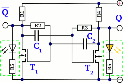
Consider that no current is running through the gate pin of a MOSFET, so when using n-channel MOSFETs instead of NPN transistors, the capacitors won't be discharged through the gate of those devices. Another problem deals with electrolytical capacitors: The threshold voltage of a MOSFET is clearly above 0.7V (which is the reverse polarity of the capacitor)! The circuit shown here operates even with high resistors R2 respectively R3, hence small capacitors can be used to get low frequencies. The charging respectively discharging current of C1 both run through R3. The charging current also runs through R4 and T1, while the discharging current runs through T2 and R1. For a visible blinking frequency of approximately 2Hz (T=0.5s): T1, T2 = 2N7000 C1, C2 = 0.33μF (don't use electrolytical types!) R2, R3 = 1MΩ R5 = 1kΩ R1, R4 = 180Ω Operational amplifier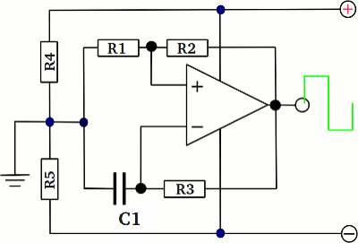
The drawing shows an astable multivibrator using a single operational amplifier. The functionality is easy to understand while considering the functional principle of a Schmitt trigger: The input of the Schmitt trigger, which is identical to the inverting input of the operational amplifier, is connected to the output of the circuit via a resistor capacitor network. While the potential at the capacitor and so at the input of the Schmitt trigger is lower than the lower threshold, the output voltage equals the positive supply voltage of the circuit. Now the capacitor gets charged via the resistor R3, until the upper threshold of the Schmitt trigger is reached. As a result, the output voltage of the operational amplifier tilts to the negative supply voltage. Now the capacitor gets discharged via R3, until the voltage across those device reaches the lower threshold of the Schmitt trigger. The output voltage of the operational amplifier tilts to the positive supply voltage and the whole process starts again. Besides the lower number of required elements, an advantage of this multivibrator is the better quality of the output signal. Even at very low switching frequencies, the slew rate of the output signal is very high and there are almost no distortions. At the video I have used: Operational amplifier: LM324N (4 in one chip) R1=47kΩ R2=12kΩ R3=1MΩ R4=R5=2kΩ C1=0.33μF For the switching time there is: [9.4a] T = 2R3C ln(1 + 2R1/R2) Where is:T - Periodical time R1, R2, R3 - Resistors C - Capacitor 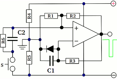
Inserting a diode in parallel to the capacitor at the previous circuit results in a monostable multivibrator. Like explained above, another capacitor (C2) and a resistor (R6) are used to create just small pulses when pushing the button. 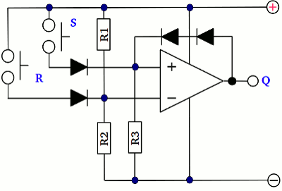
A flip-flop composed of a single operational amplifier. <<< RC circuit Pulse-width modulation >>> News The Project Technology RoboSpatium Contribute Subject index Archives Download Responses Games Links Gadgets Contact Imprint |
|
|