|
|
|
|
News The Project Technology RoboSpatium Contribute Subject index Download Responses Games Gadgets Contact <<< Diode Java-Applet Bipolar junction transistor >>> Bipolar junction transistorThe video about bipolar junction transistorsYou can find the source code of the Java program at the download section. DesignBipolar junction transistors ( BJT ) consist of a sandwich of variably doped semiconductor materials. The order is PNP or NPN. A NPN transistor is made of two layers of N-doped material with a middle layer of P-doped material, while the middle layer of an PNP transistor is made of N-doped material and it is embedded in a sandwich of P-doped material. There are electrical connectors at all three layers of the device: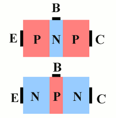
The upper drawing shows a PNP bipolar junction transistor. All three layers can be attached to a voltage source. The pins are called Emitter (E), Collector(C) and Base (B). The lower drawing shows a NPN Transistor. Transistor without being attached to a voltage source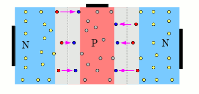
There are two P/N junctions inside of a bipolar junction transistor. Like explained at the chapter about diodes, a depletion layer is formed around the contact area by recombination of extra electrons and holes. In summation, the two N-doped layers become positively charged, while the P-doped middle layer (base) becomes negatively charged. The (immobile) charges are located near the junction and not equally distributed over the whole crystal (see chapter diodes). Yellow = pentavalent impurity atoms (e.g. phosphorus) Light blue = trivalent impurity atoms (e.g. aluminum) Blue = negatively charged impurity atoms Red = positively charged impurity atoms Attaching voltage to emitter and collector
Let's attach the emitter to the negative and the collector to the positive terminal of a DC voltage source. This will result in the following situation. Electrons are injected into the crystal at the emitter and they are extracted at the collector, by what additional holes are created at this area of the transistor. Those charges move around freely inside of the accordant layer. The electric field of the voltage source is pointing into the same direction as those of the right depletion layer, by what those zone is growing. The electric field of the left depletion layer is weakened by the field of the voltage source, hence electrons start diffusing into the P-doped layer. In here, the electrons recombine with holes, by what some of the movable charges vanish during recombination processes. The number of immobile charges is decreasing. Thus, the left depletion layer is growing, too, until no more electrons can reach the middle layer. As soon as the state of equilibrium is reached, the middle layer is more negatively charged than before. Large blue = electrons Large red = holes How to make the emitter collector line conductiveLet's have a closer look at the situation inside of the transistor while it is attached to a voltage source between emitter and collector: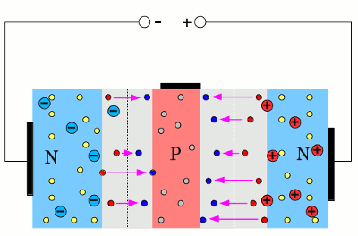
The electrons have to pass two depletion layers to be able to move from the emitter to the collector. Energy has to be applied to the electron to move it from the emitter to the point shown at this drawing. From this point, the electron is pulled to the collector by the electric field of the voltage source and those of the right depletion layer. The thermal energy of the electrons is not sufficient to move electrons from the emitter to this point. Hence, no electrons can diffuse from the emitter to the collector. No electric current is running from the emitter to the collector. Attaching voltage to the base pin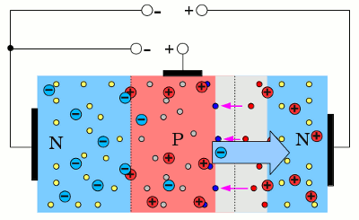
By connecting the base pin to the voltage source, electrons are extracted from the middle layer of the transistor, by what additional holes are created. The situation at the left P/N junction is the same as inside of a forward biased diode. Those depletion layer is weakened by the voltage attached to the middle layer, by what electrons can diffuse from the emitter to the base. The right depletion layer is weakened slightly by the additional holes inside of the middle layer. The barrier is now low enough that electrons can diffuse deep enough into the right depletion layer to reach the point at which they are pulled to the collector by the electric fields inside of the transistor. Thus the electrons can now move from the emitter to the collector. The transistor became conductive across the emitter-collector line. AmplifyingA voltage has to be attached to the base pin to switch the left P/N junction to forward polarity. That's necessary to facilitate the movement of electrons from the emitter to the collector. To keep the left P/N junction in conductive mode, electrons are moving from the emitter to the base pin respectively holes are moving from the base to the emitter. A current is running from the emitter to the base as well as from the emitter to the collector. The ratio of the base current to the collector current is called gain:Where is: β - gain, IB - Base current, IC - Collector current In praxis, the gain of a transistor should be as high as possible. The thicker the p-doped base region, the higher the probability that an electron hits a hole on it's way from the emitter to the collector. Electrons that recombine that way with a hole have to be replaced by the base current. If the P-doped layer becomes too thin, electrons can diffuse through those layer even without a base voltage applied to the transistor - the barrier is too weak. The number of holes inside of the p-doped layer increases with the concentration of impurity atoms. The base current increases with an increasing number of holes, too, because once again the probability becomes higher that an extra electron hits a hole. If the concentration of impurity atoms is too low, the barrier gets weakened and a current is running from the emitter to the collector even without a base current. <<< Diode Java-Applet Bipolar junction transistor >>> News The Project Technology RoboSpatium Contribute Subject index Archives Download Responses Games Links Gadgets Contact Imprint |
|
|