|
|
|
|
News The Project Technology RoboSpatium Contribute Subject index Download Responses Games Gadgets Contact DopingThe video about dopingYou can find the blender files, used to create the animated sequences at the column download. Crystalline defectsAt the previous chapter, the crystal lattice of silicon has been discussed. Each of the silicon atoms forms four covalent bonds with the neighboring atoms. All valence electrons are tightly bonded to their atoms resulting in the absence of electrical conduction. To create freely moving charges inside of silicon, the regular configuration of the crystal lattice has to be disrupted.P-type semiconductorThe conductivity of pure silicon can be increased by introducing impurity atoms, meaning atoms with a different atomic number, into the crystal lattice. The process of introducing those impurities is called doping, the introduced element is called dopant. Aluminum is a common material used for the doping process of silicon crystals. Aluminum is placed at the same period as silicon, but at the 13th group of the periodic table. The electron configuration is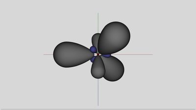
sp2-hybridization of aluminum: Three unique orbitals are the result of the hybridization process. The three hybrid orbitals are arranged with the maximum angle between the symmetry axes. The angle between the Grey painted, large drops is 120 degrees and they are arranged in a plane. The also painted third component of the p-orbital is empty and so it just exists hypothetical. 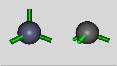
The angle between the orbitals - symbolized by the green sticks - is not a fixed value. Energy is needed to twist the orbitals, but spending those potential energy is counterbalanced by the higher gain of energy while forming covalent bonds. The angle between the orbitals of the hybridized aluminum atom is decreasing to 109.5 degrees, which is the tetrahedral angle between the atoms in a silicon crystal. The critical difference between a silicon and an aluminum atom is the number of valence electrons. There are only three valence electrons inside of the outermost shell of aluminum, hence the aluminum atom is forming only three covalent bonds with the neighboring silicon atoms. Because of the fact that silicon atoms have four valence electrons, one electron of one silicon atom remains unsatisfied. Those absence of an electron in a covalent bond is called electron hole. The energy level of the unsatisfied electron is significantly below the conduction band, so it can't move freely inside of the crystal lattice and is still located at the silicon atom. Nevertheless the conductivity of the silicon is increasing while doped with aluminum atoms. The electron hole can move through the crystal lattice: 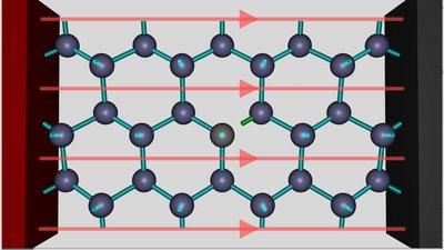
An aluminum atom is inserted into the crystal lattice of silicon. As you can see, all three valence electrons of the aluminum atom form covalent bonds with the silicon atoms next to it. The fourth valence electron of one close-by silicon atom at the right of the aluminum atom is unsatisfied. That's the place of the electron hole. The doped silicon crystal is connected to a DC voltage source. The red colored positive terminal is connected to the left of the crystal, the black colored negative terminal to the right side. 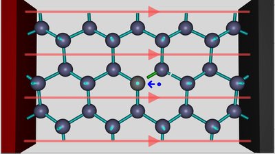
The electric field of the voltage source, visualized by the red field lines, is pulling the negatively charged electrons to the positive terminal. If the strength of the electric field increases, an electron moves from the silicon atom at the right side of the hole to the aluminum atom at the left side of the hole. 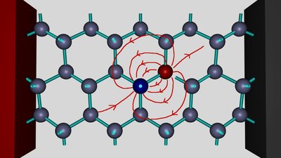
This process leads to the formation of a negatively charged aluminum ion. Like noted while talking about the orbitals of the aluminum atom, one component of the p-orbital is empty and so the additional electron can enter this orbital. Now the aluminum ion can form four identical sp3 hybridized orbitals and so four covalent bonds, resulting in a very beneficial electron configuration. By adding the electrons shared with the silicon atoms, there are eight valence electrons inside of the electron shell, which is the electron configuration of Argon, the noble gas which is located in the period of aluminum. Forming four covalent bonds inside of the electric field leads to this stable electron configuration and so to a lower energy level of the whole system. Between the aluminum and the silicon ion, the field is running contrary to the field of the voltage source, hence the external field is weakened. To the left and to the right of these two ions, the action of the external field is enforced slightly. 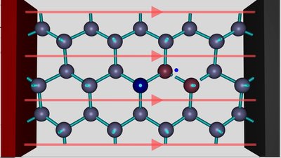
The electron hole is now located between the two silicon atoms to the right of the aluminum ion. This is the weak point inside of the crystal lattice, now. An electron is moving from the right silicon atom to the silicon ion, according to the action of the electric field. The reverse process - meaning the movement of an electron from the left to the right is inhibited by the action of the electric field caused by the voltage source AND the field of the two ions. If the electron is located between the two silicon atoms, the movement to the left is favored by the field of the voltage source. Once more the hole is moving to the right. This process continues until the negative terminal of the voltage source is reached. 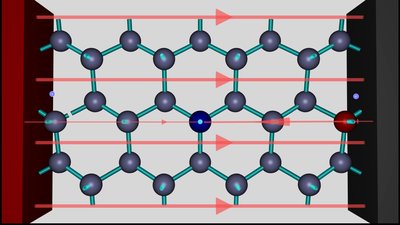
If the hole has reached the negative terminal of the voltage source, one electron is injected into the crystal lattice and simultaneously another one is extracted at the positive terminal. The balance of charges is kept constant and the hole is jumping from the negative to the positive terminal. 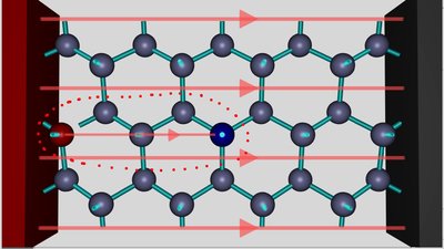
The electric field caused by the two ions is now pointing into the same direction as those of the voltage source, hence the external field is enforced between them. Nevertheless the electrons still move from the atom at the right side of the hole to the silicon ion at the left side of the hole. As from now the electron hole is to the left of the negatively charged aluminum ion, which repels the electrons. The hole is still moving from the left to the right. As soon as the electron hole and so the positively charged silicon ion has reached the position next to the aluminum ion, the electric field caused by the ions and the external field is at its maximum, hence an electron is moving from the negatively charged aluminum ion to the positively charged silicon ion. The electron hole has reached it's initial position and there are no ions inside of the crystal lattice. One electron has been transfered from the negative to the positive terminal of the voltage source and the process starts again. The electron which exits the crystal lattice at the positive terminal is different from those which entered the crystal at the negative terminal. During each step of the process another electron is moving into the hole. It seems like a positive charge is moving from the left to the right in course of the process, thus from the positive to the negative terminal. Like discussed, the positively charged silicon ions rest at their position and only the electrons move between close-by atoms from the right to the left, thus from the negative to the positive terminal. The aluminum atom is negatively charged almost during the whole process. Only if the electron hole has reached the position left to the aluminum ion, it is handing the additional electron to the close-by silicon ion, while gaining another electron from the atom to the right side immediately. It seems like the negative charge is resting at the position of the aluminum atom. The aluminum atom acts like a electron acceptor. The mechanism is called hole conduction or P-type conduction (P = positive). Adding atoms of the 13th group of the periodic table into the crystal lattice of silicon is called P-type doping. N-type semiconductorAnother possibility to increase the conductance of semiconductors is adding atoms of the 15th group of the periodic table, like phosphorus. The electron configuration of a neutral atom at it's ground state is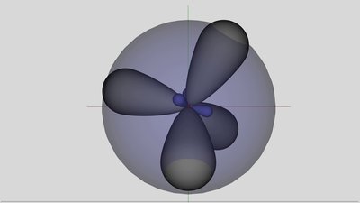
sp3 hybridized phosphorus atom. The "supernumerous" electron is located at the 4s-orbital, drawn translucent. The "supernumerous" electron of the phosphorus atom can't enter the 3s or 3p-orbital, neither at the phosphorus atom nor at one of the silicon atoms, because they are already occupied by the maximum number of electrons possible. The only place left is at the next orbital, which is the 4s orbital. One single valence electron is a very unfavorable configuration, hence the electron is just loosely bond to the phosphorous atom. The energy level of this electron is close to the conduction band. Only a small amount of energy is needed to promote electrons across the band gap to the higher electron conduction energy level. Those energy can be provided by thermal movement (heat) or by an electric field. If the electron is lifted into the conduction band, it can move about in the crystal lattice relatively freely and it facilitates conduction in the presence of the electric field. 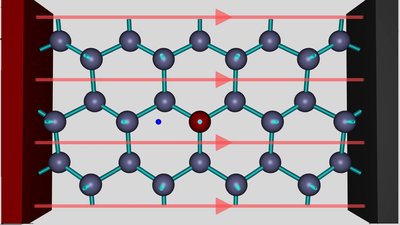
A free electron and a positively charged phosphorus atom is created inside of the crystal lattice. The electron is moving to the left, driven by the electric field (red field lines) of the DC voltage source. Adding atoms of the 15th group of the periodic table into the crystal lattice of silicon is called n-type doping. N means free moving negative charge is placed in the crystal lattice. A dopant atom forming a n-type region inside of a semiconductor is called electron donor or donor. Technology of dopingSemiconductors of the 14th group (called group IV semiconductors), are usually doped with impurity atoms of the 13th or 15th group. Atoms acting as electron donors are arsenic, phosphorus and antimony, electron acceptors are boron, aluminum, indium or gallium.There is one impurity atom between 107 (normal) and 104 (strong) silicon atoms in N-type material. At P-type material, the number of silicon atoms per impurity atom is 106 (normal) respectively 104 (strong). News The Project Technology RoboSpatium Contribute Subject index Archives Download Responses Games Links Gadgets Contact Imprint |
|
|