|
|
|
|
News The Project Technology RoboSpatium Contribute Subject index Download Responses Games Gadgets Contact SiliconThe video about siliconPropertiesSilicon is making up more than 25 percent of the Earth's crust by mass, mostly in the form of silicon dioxide or silicates and very rarely occurs as the pure free element in nature. It is placed at the 14th group of the periodic table. along with the elements carbon, germanium, tin, lead and the radioactive element ununquandium. All of those chemical elements feature four electrons in the outermost shell, available for covalent chemical bonding. Those elements are called to be tetravalent.The atom number of silicon is 14, meaning a neutral atom features 14 protons inside of it's nucleus and the same number of electrons inside of the atomic shell. The number of neutrons fluctuates between 14 and 16, at non-artificial silicon resulting in an atomic weight of 28.0855 u. Orbital hybridizationThe currently accepted theory of the atomic shell is the so called atomic orbital model. Based on mathematical functions describing the wave-like behavior of either one electron or a pair of electrons in an atom, orbitals can be calculated. Those orbitals represent a space, the electrons can be located in with a given probability.The electron configuration of silicon is: The four valence electrons of the outer electron orbitals are located at the 3s-orbital (2 electrons) and the 3p-orbital (2 out of six electrons). That's for true as long as the silicon atom is insulated. When forming covalent bonds with other atoms, the 3s and the 3p orbitals are mixed with each other and form new hybrid orbitals: 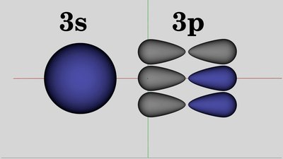
Four uniform hybrid orbitals are formed out of the ball socket shaped 3S orbital and the drop shaped 3p orbital. 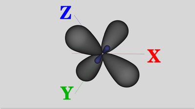
3D drawing of hybrid orbitals: The four hybrid orbitals are arranged in such a way that the distance between the orbitals is maximized. The resulting angle between the Grey colored, larger drops of the hybrid orbital is 109.45 degrees. Ball and stick modelTo display the 3D position of atoms and the chemical bonds between them, the "ball and stick model" is often used. In doing so, the atoms are represented by spheres and they are connected by rods, representing the bonds. The angles between the rods are the same as the observed angles between the bonds of the according atoms.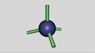
Ball-and-stick model of a silicon atom: The four rods, representing the valence electrons are arranged with an angle of 109.45 degrees between each other. This angle is also called tetrahedral angle, because it is the angle between the segments joining the center and the vertices of a tetrahedron, which is a body having 4 corners. Crystal structure of siliconLike carbon and germanium, silicon crystallizes in a diamond cubic crystal structure, too. Each of the four valence electrons forms a covalent bond to another silicon atom.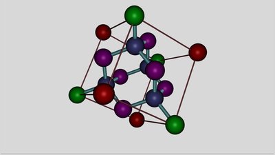
Face-centered cubic crystal structure: A cube can be placed inside of the crystal structure in such a way that there is one atom at each vertex and one atom at the center of each face of the cube. The four red marked atoms are placed at the vertices of the cube without being connected directly to the atoms in the center of the cube. The four green marked atoms at the vertices are directly connected to the atoms at the center of the cube. The six magenta colored atoms are arranged at the center of the six square faces. The spacing between the centers of two atoms along a covalent bond is 0.5430710 nm in a silicon structure and 0.154 nm in a diamond crystal. Space-filling modelYou can't see the atoms of the crystal lattice with your eyes and even the strongest microscopes are not able to display the structure directly. The surface of the crystal lattice can be scanned by using an atomic force microscope. The thereby generated pictures are not comparable to the ball and stick model used here. Closer to the reality is the so called calotte-model or space-filling model, where the atoms are represented by "full size" spheres. The bonds conform to the overlapping areas of the single spheres.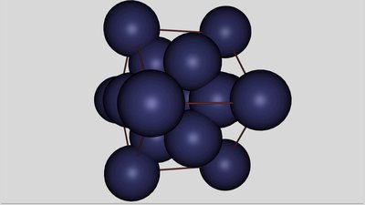
Calotte-model of a face-centered cubic crystal structure 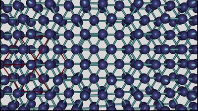
Ball-and-stick model of silicon, diamond or germanium. 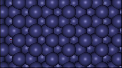
Calotte-model of silicon, diamond or germanium. News The Project Technology RoboSpatium Contribute Subject index Archives Download Responses Games Links Gadgets Contact Imprint |
|
|