|
|
|
|
News The Project Technology RoboSpatium Contribute Subject index Download Responses Games Gadgets Contact <<< Doping Java-Applet Diode >>> DiodeThe video about the chapterYou can find the blender files, used to create the animated sequences in the column download. DiffusionAt the previous chapter the "migration" of electron holes inside of a p-type semiconductor while exposed to an external electric field has been discussed. Even without an external field, the holes can't be located at a fixed place. The energy level of the covalent bonds between the substituted atom (aluminum) and the close by silicon atoms is identical, hence it doesn't matter where the hole is located. No energy is needed to push the hole around the impurity atom. To move the hole away from the substituted atom, an electron has to be transfered from a neighboring silicon atom to the impurity atom. During this procedure a negatively charged impurity ion and a positively charged silicon atom is created. Energy is needed to crack the bond between two silicon atoms and to separate the electron from one silicon atom. There is a gain of energy while the electron is entering the impurity atom and while one more covalent bond is formed between those atom and the fourth silicon atom. The energy difference of the whole process depends on the used materials and can be positive as well as negative. If there is just a low energy difference, the process can run into both directions, induced by thermal energy (heat). The hole can migrate from the impurity atom. The movement of the hole is irregular and it can also move back to the aluminum atom. The random movement of the holes is called diffusion: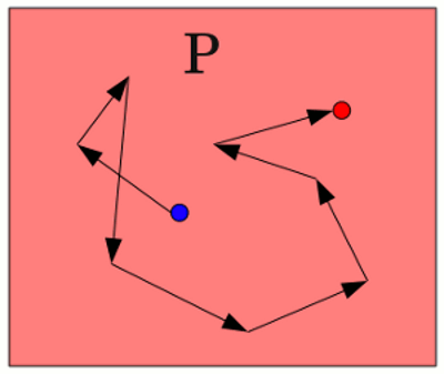
A negatively charged aluminum ion (blue) and a positively charged silicon ion (red) was created inside of a p-doped silicon crystal. The negative charge is connected to the aluminum atom, hence it is immobile. The positive charge is moving around, induced by the exchange of electrons between the silicon atoms. By exposing the crystal lattice to an electric field, a movement of the charged particles into the direction of the field is induced. The movement according to the electric field is called drift. The drift of the electrons is always superposed by the irregular movement of the diffusion. Inside of a n-type semiconductor, the loosely bond electron of the impurity atom can be lifted into the conduction band, hence it can move relatively freely around the crystal lattice. The movement of the electron is irregular, too. An applied electric field gives the random motion a net velocity according to the direction of the field, which is called drift velocity. P-N junctionIf a P-type and a N-type semiconductor are joined together in very close contact, holes diffuse from the P-type region into the N-type region and electrons diffuse into the opposite direction. Whenever a hole meets one of the free electrons, both charges recombine. The electron enters the vacant place between two silicon atoms resulting in an additional covalent bond. Inside of the N-type region, positively charged (immobile) donor ions are left behind and negatively charged (immobile) acceptor ions are created inside of the p-type region. As a consequence of the process, an electric field is generated between the now positively charged N-type region and the negatively charged P-type region. The electric field opposes the diffusion process of further holes respectively electrons between the regions. Electrons are pulled back to the N-type region, holes are pulled back to the P-type region inside of the field. At the state of equilibrium, the diffusion process that tends to generate more charged particles is balanced by the electric field of the already established charged ions. The potential difference between the two regions at the state of equilibrium is called built-in potential Vbi. The region nearby the contact area becomes charged, forming the space charge region, junction region or depletion layer. The charge of the impurity atoms inside of the region is fixed and can't be removed by diffusion processes.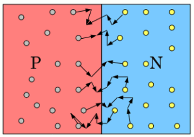
Diffusion and recombination of electrons and holes at a PN junction. 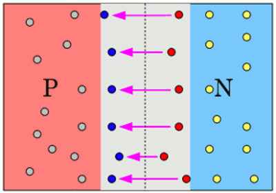
Holes of the P-type region and electrons of the N-type region recombine. There are no mobile charge carriers inside of the Grey painted region. The electric field of the ions inhibits the exchange of charge carriers between the N-type region and the P-type region. Yellow = pentavalent impurity atoms (e.g. phosphorus) Light blue = trivalent impurity atoms (e.g. aluminum) Blue = negatively charged impurity atoms Red = positively charged impurity atoms The electric field of the depletion layer can be influenced by an external field of a voltage source. Let's connect the P-type region to the positive terminal of a DC voltage source and the N-type region to the negative terminal: 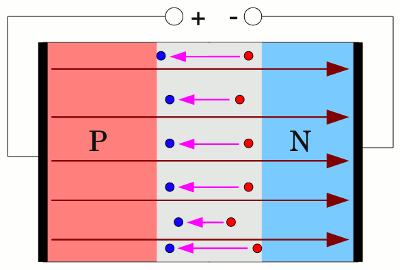
The electric field of the voltage source is running contrarious to those of the depletion layer. 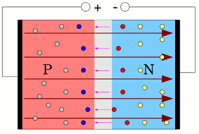
The electrons of the N-type region and the holes of the P-type region are pushed towards the junction which reduces the width of the depletion layer and lowers the barrier in potential. Electrons can drift through the weakened field of the space charge region from the N-type region to the P-type region and holes into the opposite direction from the N-type region to the P-type region. If the voltage output is increasing, the electric field of the contact area is canceled out and a current is running through the device without a barrier. The electrons entering the P-type region at the junction recombine with the holes, which are the majority carriers of this region. The average length an electron travels through the P-type material before recombining is called the diffusion length, and it is typically on the order of microns. Let's invert the polarity of the voltage source. The negative terminal is connected to the P-type region and the positive terminal to the N-type region. The electric field of the voltage source is pointing into the same direction as those of the depletion layer from now on. The field is not weakened and the diffusion respectively drift of electrons and holes is not facilitated. Electrons are injected into the P-type region, by what further holes are removed through recombination processes. At the N-type region, electrons are removed by the voltage source, hence they are pulled away from the junction. The voltage barrier increases and the depletion layer is widened. 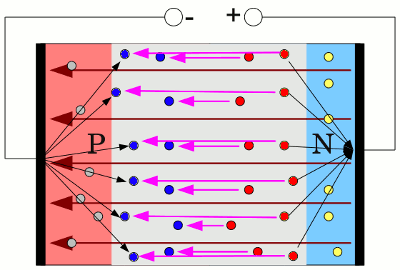
Electrons are injected into the P-type region, removing holes by recombination processes. At the N-type region, electrons are removed by the voltage source. Both processes widen the depletion layer around the junction. <<< Doping Java-Applet Diode >>> News The Project Technology RoboSpatium Contribute Subject index Archives Download Responses Games Links Gadgets Contact Imprint |
|
|