|
|
|
|
News The Project Technology RoboSpatium Contribute Subject index Download Responses Games Gadgets Contact <<< Amplifying ICs Read switches >>> DemultiplexerThere is no Video about demultiplexers available, yet.Leave a comment, if you have ideas of what to show in that video (besides the things already mentioned on this page).OverviewIn this chapter you can read about:
Addressing
You often have a need to switch more loads than GPIOs are available. In the chapter about switching an LED matrix, we already got to know a way to do just that. With the help of demultiplexing, however, the number of loads to be controlled can be increased even further. This method uses the GPIOs to output addresses in binary format. I explained how counting in the dual system works in the chapter about computing. The quantity of numbers that can be represented is 2n, where n corresponds to the number of digits, in our case the number of GPIOs. With 4 GPIOs, 0000 = 0 0001 = 1 0010 = 2 0011 = 3 0100 = 4 0101 = 5 0110 = 6 0111 = 7 1000 = 8 1001 = 9 1010 = 10 1011 = 11 1100 = 12 1101 = 13 1110 = 14 1111 = 15 By means of an appropriate wiring, one of these numbers can now be assigned to each of the loads. The loads get an individual address. Logic gates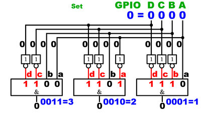
Logic gates are used to assign an address to a load. This requires AND gates as well as NOT gates. Since an address consists of 4 bits, quadruple AND gates are required to select a special load. For each "0" in the binary number of the address, a non-gate must be connected at the input of the gate, the positions with a "1" are directly connected to the GPIO pins. The hardware address of the right gate is "1", which corresponds to the binary number "0001", which means that NOT gates are required at the inputs "b", "c", and "d". For the middle gate with the decimal address "2" ("0010" as a binary number) there are NOT gates at the inputs "a", "c" and "d", on the left gate with the decimal address "3" ("0011" as a binary number) NOT gates are required at inputs "c" and "d". In the initial state, all 4 GPIOs are LOW ("0"). The NOT gates invert the "0" at their inputs to a HIGH signal ("1") at their outputs. Thus e.g. in the middle AND gate the inputs "a", "c", and "d" are HIGH ("1"). None of the three AND gates have a HIGH signal at all inputs, so all outputs are LOW. 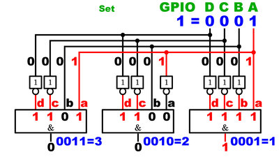
Now, the GPIOs represent address "1" ("0001"): A HIGH signal is thus present at input "a" on the right AND gate. A LOW signal from the GPIOs "B" to "D" is sent to the inputs "c" to "d". Since NOT gates are connected at input "c" to "d", these convert the signals to HIGH level, which means that all 4 inputs of the right AND gate are HIGH, which means that the AND condition is met and the output of the gate goes to HIGH signal. At the middle (inputs "a" and "b") and left gate (input "b") there are still inputs with a LOW signal, which is why the AND condition is not fulfilled, here. 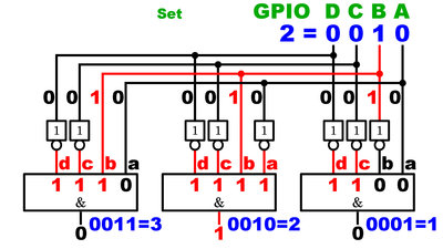
Address "2" ("0010") is represented by the 4 GPIOs: At the right AND gate, the HIGH signal from GPIO "B" is converted into a LOW signal at input "b", the LOW signal from GPIO "A" is sent directly to input "a". The AND condition is no longer fulfilled, the output goes to LOW. Now the AND condition is fulfilled for the middle gate. The LOW signal from GPIO "A" is converted by the NOT gate at input "a" into a HIGH signal, the HIGH signal from GPIO "B" is passed directly to input "b" and the LOW signals from the GPIOs "C" and "D"are converted from the NOT gates to HIGH signals at inputs "c" and "d". The output is on a HIGH signal. With the left gate, input "a" is LOW, accordingly the output remains on LOW signal. 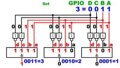
The next address given by the 4 GPIOs is "3" ("0011"): At the right AND gate, the LOW signal at input "b" ensures that the AND condition is not met, the output remains LOW. At the middle gate, input "a" is LOW, which breaks the AND condition. The output goes back to LOW signal. The HIGH signals of GPIO "A" and "B" are forwarded directly to the left gate, while the LOW signals of GPIO "C" and "D" are converted to HIGH signals via the NOT gates. If the GPIOs output the address "3", the output of the left gate goes HIGH. 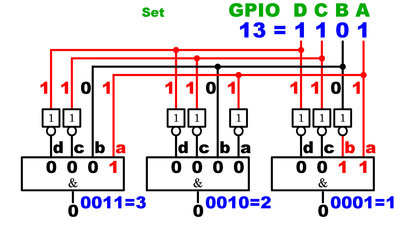
For none of the other addresses from 4 to 15, one of the outputs of the three gates goes HIGH. At least one of the inputs "a" to "d" is always on LOW signal. Here address "13" (dual number "1101") is represented by the GPIOs. Switching delay
Signals are always forwarded with finite speed. If the states of the GPIOs change, this does not have an immediate effect nor are all inputs of the AND gates affected at the same time. Especially at the NOT gates a noticeable time elapses until the signal is inverted. In this figure the address "2" (dual number "0010") is represented by the GPIOs again. Now, the GPIOs switch over... 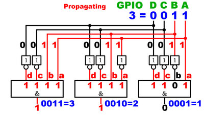
... to address "3" (dual number "0011"), here you can see the state that results from the delay at the NOT gates: When changing from "2" to "3", only the state of GPIO "A" changes from LOW to HIGH. The change in state is passed on to input "a" of the left gate (more or less) immediately, which means that the AND condition is fulfilled at this gate and its output goes to a HIGH signal. The signal change from GPIO "A" to input "a" of the middle AND gate is delayed by the NOT gate, so that the AND condition remains (still) fulfilled on this. In this transition phase, two AND gates are switched on at the same time! 5 GPIOs for 4-Bit addresses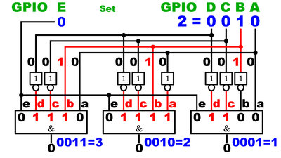
With the help of another GPIO, the AND gates can be blocked when the addresses change. AND gates with five inputs are now required. Again address "2" is represented by the GPIOs. If GPIO "E" is LOW, the output of the middle (and all other) AND gates is also LOW. 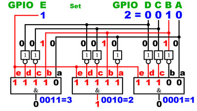
The middle AND gate only goes HIGH at the output when GPIO "E" is also set to HIGH signal. GPIO "E" is called data input, or strobe.
Before switching to the next address, GPIO "E" is set to LOW, which means that all AND gates are blocked, since input "e" breaks the condition at the latest. The output of the middle AND gate goes LOW again. 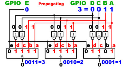
Thus, even in the transition phase when switching to address "3" (dual number "0011"), there is no undesired activation of two AND gates. 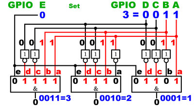
If the signal of the new address is present at all inputs,... 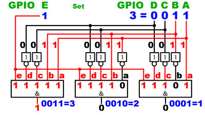
...the left AND gate can now be switched on via GPIO "E" if required. 5 GPIOs are required with the demultiplexer shown here to switch up to 16 loads. With a 4x4 LED matrix, 8 GPIOs are needed. With the demultiplexer, however, there is no way to switch multiple loads at the same time. Only one AND gate can be activated at a time. With AND gates having 6 inputs, up to 32 loads can be switched, with 7 input AND gates 64 loads and so on... The whole thing as picture sequenceMake sure that Javascript is activated in your browser to click through the sequence.The example shows the total circuit logic for the addresses "6" ("0110"), "7" ("0111") and "13" ("1101").
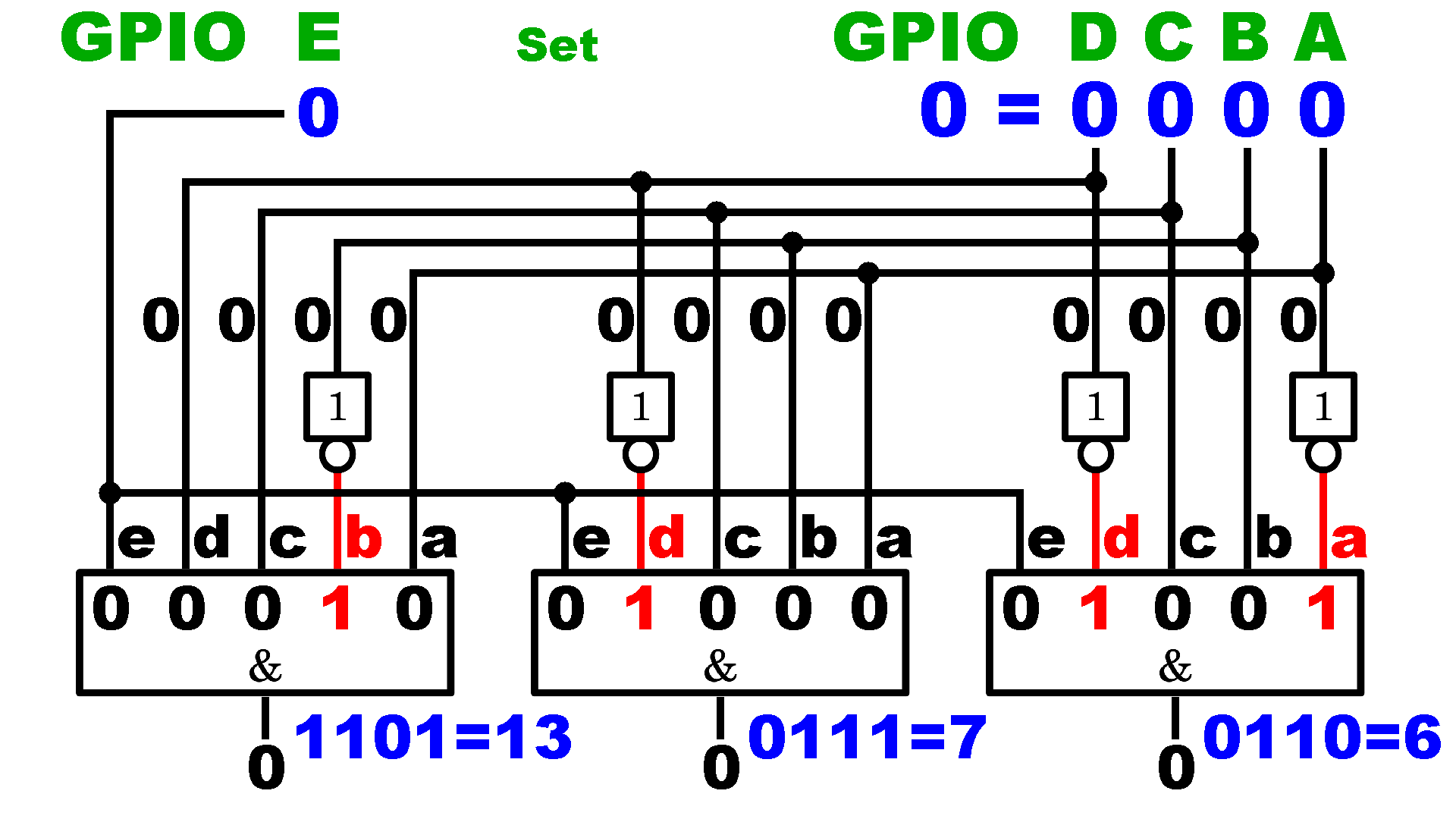
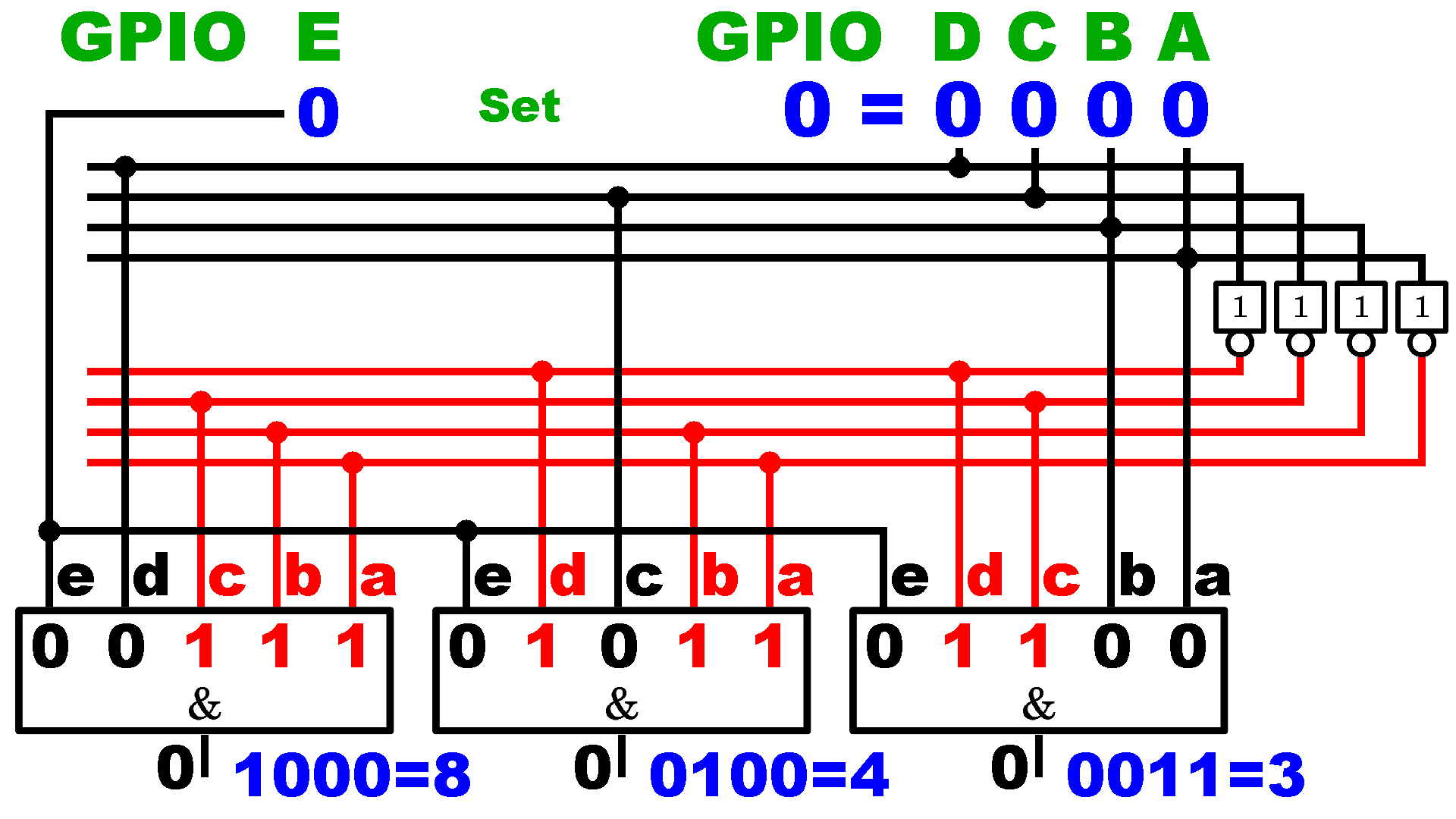
Fewer NOT gatesIt is sufficient to install only 4 NOT gates directly at the four address inputs. In the example shown here with the binary numbers "1000" (=8), "0100" (=4) and "0011" (=3), according to the previous scheme, 8 NOT gates would be required for these three addresses alone.
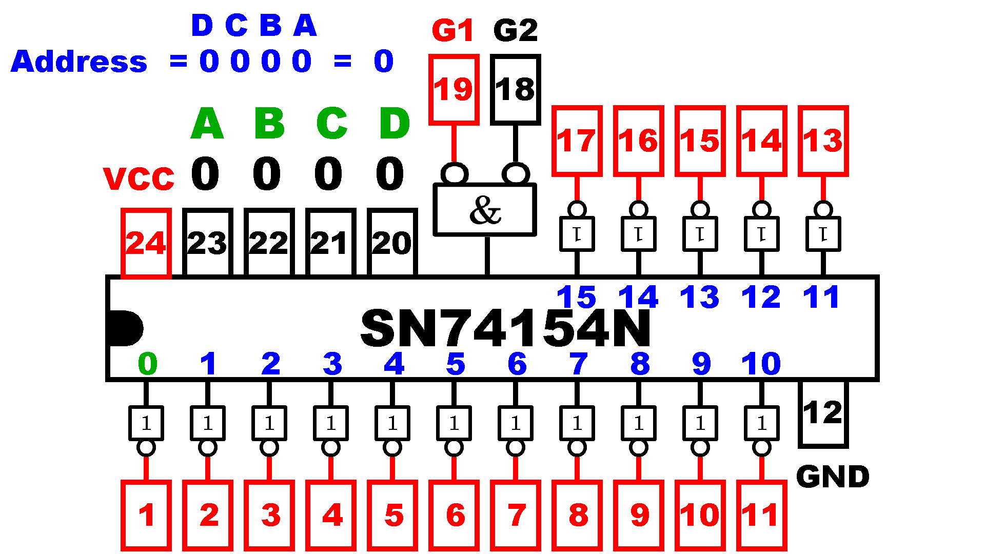
SN74154N 16 channel demultiplexer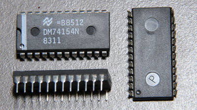
A practical example of a 16-channel demultiplexer with 5V supply voltage is the 74154N shown here. According to the data sheet, the time span from changing the address at the 4 inputs (pins 20 to 23) to reaching the outputs is a maximum of 36 nanoseconds. The chip is designed as a sink current driver IC (details in the chapter about amplifier ICs) for up to 16mA per channel. This means that loads must be connected between the positive supply voltage and the outputs of the chip and are therefore deactivated when a HIGH signal is present at the corresponding output. The chip is an Active LOW type. The chip has 2 strobe inputs, both leading to an additional AND gate through NOT gates. With sink current drivers, the "reverse" logic applies to the outputs. This means that, compared to the examples above, the output are LOW when being activated and HIGH if being deactivated. 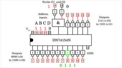
Here the address "7" (dual number "0111") is selected at the inputs. It should be noted that the inputs "A" to "D" are arranged from left to right in the drawing. G1 is HIGH, G2 is LOW, which means that only the right input of the AND gate is HIGH (through the NOT gate). The AND condition is not met and therefore there is a LOW signal at the output and thus at the same time at at least one of the five inputs of the AND gates at the outputs. The AND condition is nowhere fulfilled and due to the NOT gates at the outputs, these are all at HIGH level. 
Now, if input G1 goes LOW, the AND condition at the strobe inputs is fulfilled by the NOT gates. This means that the fifth input of the AND gate at output "7" also goes HIGH because of the fulfilled AND condition. This signal is inverted by the NOT gate, making the output with address "0111" the only one to go LOW. The addressed output only goes LOW if both inputs G1 and G2 are LOW. If G1 or G2 (or both) is HIGH, the AND gate at the input is LOW, which means that all outputs go HIGH. Thus G1 can be used as an inverted data input and G2 can be used to activate or deactivate the circuit. If there is a HIGH signal at G2, the demultiplexer is blocked, all outputs are forced to HIGH, independent from the state of G1. The addressed output can only be switched via G1 if G2 is on LOW signal. G2 is therefore the Not Enable Pin. The demultiplexer is deactivated with a HIGH signal at G2 (=not activated). Animation SN74154NThe animated version shows the states of the outputs depending on the states of the inputs and should therefore help to answer all remaining questions.
Sourcing partsWhen buying components via the affiliate partner links I have listed in the table (or through the banners on my pages) you help to keep my my projects going - many thanks!Clicking on the links does not mean you have to buy - you can simply browse through the pages ;-) Of course, supporting my freely accessible educational platform without shopping but by making a donation or becoming a Patreon also works. Many thanks to everyone who already sent me an obol! If you know more commonly available demultiplexer ICs, please leave a comment on this page.
<<< Amplifying ICs Read switches >>> News The Project Technology RoboSpatium Contribute Subject index Archives Download Responses Games Links Gadgets Contact Imprint |
|||||||||||||||||||||
|
|