|
|
|
|
News The Project Technology RoboSpatium Contribute Subject index Download Responses Games Gadgets Contact <<< Demop board H-Bridge Demultiplexer >>> Amplifying ICsThere is no Video about amplifying ICs available, yet.Leave a comment, if you have ideas of what to show in that video (besides the things already mentioned on this page).OverviewIn this chapter you can read about:
Operational amplifier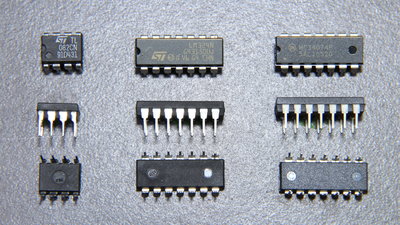
The operational amplifier is a very common device that is available in many variants as an integrated circuit on a chip. Operational amplifiers are rarely used directly for switching high currents, but are commonly used as a preamplifier stage, level converter or inverting buffer. The working principles of these circuits is treated in the chapter about operational amplifiers. This page is only about amplifying digital signals. The photo shows ICs with two and four operational amplifiers per chip. 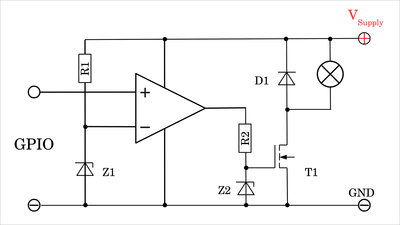
In this circuit diagram, an operational amplifier is used as a preamplifier or level converter. The voltage divider at the input, composed of R1 and Zener diode 1, determines the "threshold voltage". An operational amplifier without feedback, as shown here, works as a comparator, which means that its output voltage is (almost) 0V whenever the voltage at the non-inverting input (labeled "+") is lower than the voltage at the inverting input (labeled "-"). The output voltage equals (almost) the supply voltage (VSupply) whenever the voltage at the non-inverting input is above that at the inverting input. These two voltages are never exactly the same in real circuits. If the difference in voltages between the two inputs is small, even the smallest variation, inevitably caused by noise, will make the output voltage jump randomly between 0V and VSupply. Since I am only treating the amplification of digital signals in this chapter, this appears only for a very short time during the transition from LOW to HIGH or vice versa from HIGH to LOW and can therefore be neglected. An advantage is that the threshold voltage, which is determined by the value of the Zener diode Z1, can be selected to be very small, so that even the 3.3V of a Raspberry Pi are suitable for operating the amplifier circuit without any problems. If the circuit is intended to be used at only a constant supply voltage, the Zener diode can be replaced by a second ohmic resistor. With a supply voltage of 12V, the resulting threshold voltage of 1.6V can be achieved with resistors of 10kΩ (R1) and 1.5kΩ. Zener diode number 2 and flyback diode D1 serve to protect the N-channel MOSFET against overvoltages, as described in more detail in the chapter about switching N-channel MOSFETs. Possible components for a supply voltage ranging from 10V to 24V at up to 30A (with very good cooling of the MOSFET): Operational amplifier: LM324N MOSFET: z.B. IRLZ34N Z1: 2V, 500mW Z2: 10V, 500mW D1: z.B. SR5100, 5A continuous current, 150A peak current R1 and R2: 10kΩ, 0.25W 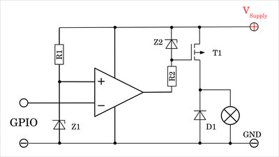
In this circuit, the operational amplifier is used as an inverting preamplifier or level converter. Whenever the GPIO is on LOW (0V), the voltage at the non-inverting input ("+") is above that at the inverting input ("-"), which means that the output voltage of the operational amplifier equals (almost) the supply voltage. The P-channel MOSFET is thus switched OFF when the GPIO is also switched OFF (on LOW signal). With a HIGH signal at the GPIO, the voltage at the non-inverting input is below that at the inverting input, which means that the output of the operational amplifier equals (almost) 0V. As can be read in the chapter about switching P-channel MOSFETs, this device is switched on whenever the gate-source voltage is negative. HIGH signal on the GPIO switches the load ON. Possible components for a supply voltage ranging from 10V to 24V at up to 19A (with very good cooling of the MOSFET): Operational amplifier: LM324N MOSFET: z.B. IRF9540 Z1: 2V, 500mW Z2: 10V, 500mW D1: z.B. SR5100, 5A continuous current, 150A peak current R1 and R2: 10kΩ, 0.25W 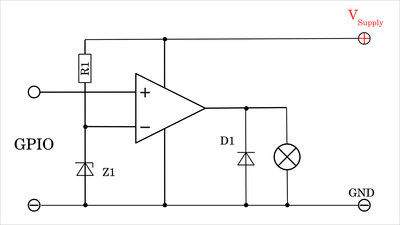
Operational amplifiers can also be used to directly switch loads. However, this is a rather exotic application, which is why the maximum output currents of the most common models are rather low and are sometimes even not listed in the data sheet. The very cheap LM324N can only switch about 30mA. Currents of up to 3A at up to 60V can handle e.g. the OPA548, which is significantly more expensive than an LM324N including an N-channel MOSFET. Possible components for a supply voltage ranging from 10V to 48V at up to 3A (with very good cooling of the operational amplifier): Operational amplifier: OPA548 Z1: 2V, 500mW D1: z.B. SR5100, 5A continuous current, 150A peak current R1: 10kΩ, 0.25W 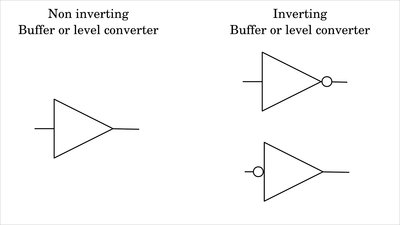
This drawing shows simplified representations of an operational amplifier, which are often part of the internal layout of integrated circuits as inverter or level converter and so often appear in the drawings of data sheets. Sink Current driver ICs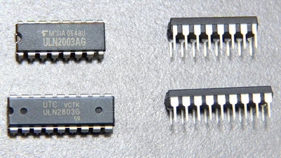
If several low power loads are to be controlled, the use of driver ICs with multiple inputs and outputs is often cheaper to buy and quicker to assemble than many small signal transistors. A good example is the ULN2803A, which can switch a total of 8 channels at a supply voltage of up to 50V with up to 500mA each. The ULN2003 features 7 channels per chip. 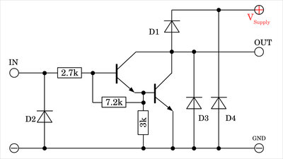
A single channel consists of a pair of NPN transistors that are connected in the so-called Darlington configuration. Part of the internal circuit are also a 2.7kΩ series resistor that limits the base current, pull-down resistors at the inputs and a protective diode (D1) at the outputs. D2 - D4 are so-called parasitic diodes, i.e. P/N junctions within the transistors, that act like diodes. 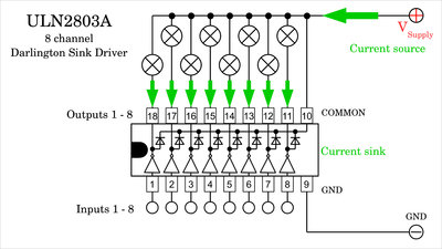
The loads to be switched are connected between the positive supply voltage (VSupply) and the outputs of the chip. The (conventional) current therefore flows from the voltage source via the load into the IC. This acts as a current sink, hence the name sink current driver. The IC is designed for 5V logic voltage, whereby a current of about 2mA flows into the inputs when the HIGH level is applied. Apart from the IC, no other components are required to switch up to 8 loads. In the equivalent circuit diagram of the chip, inverting operational amplifiers are drawn. When a LOW signal is present at the input, the supply voltage is present at the corresponding output. Since the load is connected between the positive supply voltage and the output of the operational amplifier, the positive supply voltage is present at both of these terminals and so no current flows. If HIGH is present at the input, the output of the operational amplifier is (almost) 0V and so (almost) the whole supply voltage drops between the connections of the load. Whenever HIGH signal is present at the input, the according output of the IC is at 0V, which switches the load ON. Source Current driver ICs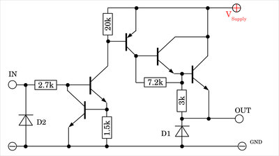
The UDN2981A is an 8-channel source current driver IC. A single channel in the core also consists of a pair of NPN transistors in Darlington configuration. However, here the Darlington transistor is switched by an additional PNP transistor. Diode D1 is integrated as a flyback diode, so that the IC is suitable for switching inductive loads. Diode D2 is a "parasitic diode". 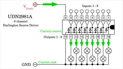
The loads to be switched are connected between ground (GND) and the outputs of the chip. The (conventional) current therefore flows out of the IC through the load to ground. The IC acts as a current source, hence the name source current driver. As with the P-channel MOSFET, the current flowing out of the chip is noted with a negative sign in the data sheet. The IC is designed for 5V logic voltage, whereby a current of less than one milliampere flows into the inputs when HIGH level is applied. Apart from the IC, no other components are required to switch up to 8 loads. Non-inverting operational amplifiers are drawn in the equivalent circuit diagram of the chip. If a LOW signal is present at the input, 0V is also present at the corresponding output. Since the load is connected between the output of the operational amplifier and ground, there is no voltage across it's terminals and so no current flows. If HIGH is present at the input, the supply voltage is present at the output of the operational amplifier, which switches the load ON. Sourcing partsWhen buying components via the affiliate partner links I have listed in the table (or through the banners on my pages) you help to keep my my projects going - many thanks!Clicking on the links does not mean you have to buy - you can simply browse through the pages ;-) Of course, supporting my freely accessible educational platform without shopping but by making a donation or becoming a Patreon also works. Many thanks to everyone who already sent me an obol! If you know more ICs or common, cheap power diodes that are good for the circuits shown in this chapter, please leave a comment on this page. <<< Demop board H-Bridge Demultiplexer >>> News The Project Technology RoboSpatium Contribute Subject index Archives Download Responses Games Links Gadgets Contact Imprint |
|
|