|
|
|
|
News The Project Technology RoboSpatium Contribute Subject index Download Responses Games Gadgets Contact <<< Amplifier Operational amplifier >>> SwitchThe video about switchesCurrent controlA switch is an electrical or electromechanical component that can interrupt the current running through an electric circuit. An electromechanical device consists at least of two electrical contacts which can be either in the state open, meaning the contacts are separated from each other, or in the state closed, meaning the contacts are touching each other. Ideally the resistance in the state "open" is infinite, while it is zero in the state "closed".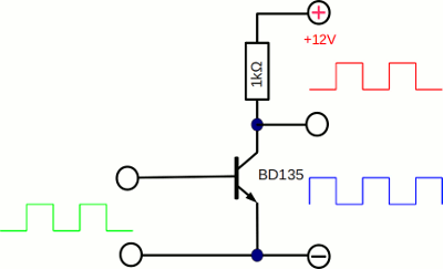
At the previous chapter we have learned that the resistance of a bipolar junction transistor can be altered by attaching a voltage to the base pin. The resistance is high (above 20MΩ) if 0V are attached to the base pin and it becomes low (clearly below 100Ω) if those voltage increases above +0.6V (NPN types) respectively decreases below -0.6V (PNP types). A transistor can conceptually open or close electric circuits by altering the emitter collector resistance from it's minimum value ("close") to it's maximum value ("open") or vice versa. Turning "off" The electric curcuit attached to the emitter collector line of a bipolar junction transistor is "open", if 0V are attached to it's base pin. The most simple circuit consists of a transistor and a load resistor. The emitter collector line of the transistor and the load resistor are forming a voltage divider. The voltage drop at the load resistor is:
  A device with a resistance similar to those of the turned off transistor is a reverse biased diode. Now the voltage drop at the diode equals approximately those at the transistor, which is half the total voltage. Nevertheless, the current running through the circuit and so the power dissipation at the load (=diode) is extremely low. Just keep in mind, that a transistor is never a perfect switch.
Turning "on"
Let's connect a LED in series to a 1kΩ load resistor to indicate the switching status of the transistor. While increasing the base voltage, the LED starts "glimming" around 0.53V, it is shining brightly at 0.60V and there is no more increase in luminosity above 0.67V. To turn the LED on, a base voltage of 0.67V has to be attached to the base pin. The resulting voltage drop at the 1KΩ resistor is 9.5V, those at the LED is 2.07V and those at the transistors emitter collector line is 52mV. A current of Another important value is the resistance of the transistors emitter collector line, which is Let's replace the LED and the load resistor by an electric motor. The base voltage is still adjusted to 0.67V however the motor doesn't turn until it is increased to 0.72V - why? Well, the ohmic resistance of the electric motor is significantly lower than those of the LED and the 1kΩ resistor, hence the voltage drop at the transistor is now 10V (remember the correlations in a voltage divider). The base voltage has to be increased to decrease the resistance of the emitter collector line. At a base voltage of 0.75V the motor is turning with the maximum rounds per minute in idle mode and we get: Voltage drop Emitter collector: 95mV Base current: 17mV / 10Ω = 1.7mA Voltage drop motor: 11.5V Current through motor: 70mA The resistance of the emitter collector line drops down to Base Voltage: 0.75V Voltage drop emitter collector: 8V Voltage drop motor: 4V Current through motor: 200mA The resistance of the emitter collector line increased to Like mentioned above, an ideal switch has no resistance while being closed, but what's the minimum resistance of our transistor? There is no value for the minimum resistance of the BD135 listed at the datasheet, but the maximum continuous base current is 500mA at a base voltage of 1V. The accordant collector emitter voltage is 2V and the maximum collector current 1.5A, by what the minimum resistance when operating with the maximum current is 1.3Ω. An input power of Keep in mind that the resistance of a transistor gets low, while it is turned "on", but it is never zero! 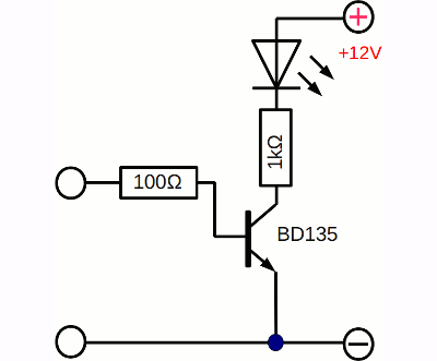
A voltage divider is rarely used at the input circuit of bipolar junction transistors. Normally there is just a single resistor switched in series to the base pin. Those resistor is forming the accordant voltage divider with the forward biased junction between base and emitter. The resistance value must meet the specifications of the transistor and the voltage of the input signal. If a base current of 50mA is required to safely turn your transistor "on" and your input signal has a voltage output of 5V, the resulting resistance value is Field effect transistorsNo input power is required to keep the switching state of a field effect transistor. If a voltage of 0V is attached between source and gate pin, JFET transistors are "closed" ("on"), MOSFET transistors are "open" ("off"). The resistance of a JFET increases with increasing gate voltage, those of MOSFETs decreases with increasing gate voltage. So the behaviour of MOSFETs is similar to those of bipolar junction transistors, however the voltage drop at the gate pin is usually greater than those at the base pin of BJTs. For example the maximum gate voltage of the IRLZ24N, an N-channel MOSFET is 16V, which would destroy all bipolar junction transistors. The "on" resistance is often listed at the datasheets of MOSFETs. The static drain to source on resistance RDS(on) of the IRLZ24N is 60mΩ at a gate voltage of 10V and a drain current of 11A respectively 105mΩ at a gate voltage of 4V and a drain current of 9A.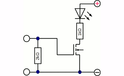
Keep in mind that the gate pin of field effect transistors must be connected to an input circuit to avoid curious behavior. There is no internal conductive path from the gate area to the source or the drain like inside of a bipolar junction transistor. The charge cumulated at the gate area can't flow off. To ensure that a N-channel MOSFET is turned "off" while not connected to an input circuit, a resistor has to be connected between gate and source, pulling the voltage level to ground (pull-down resistor). 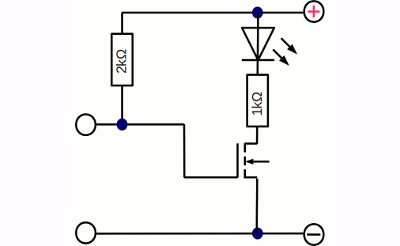
By connecting a resistor between gate and the positive terminal of the supply voltage, the N-channel MOSFET is turned "on" while not connected to an input circuit (pull-up resistor). Always use high resistance devices as pull-up respectively pull-down resistors to keep the input power low, because now a current is running trough the resistor even while the switching status of the FET is not altered. Switching frequencyChanging the state of a transistor always takes some time. When turning a transistor "on", the voltage drop at the emitter collector line drops from (nearly) the supply voltage of the circuit to (nearly) 0V. Vice versa the voltage is increasing from 0V to the value of the supply voltage while the transistor is turned "off". The maximum rate of change of a signal (voltage drop) is called slew rate. It is usually expressed in units of V/μs. Sometimes the rise time is listed at the datasheets of transistors instead of the slew rate. So if the voltage at the emitter collector line rises from 0V to 12V in 100ns, the average slew rate is 120V/μs.The maximum switching frequency of a transistor is ruled by the time needed to turn a transistor "on" and "off" again. Assuming a slew rate of 100V/μs, the maximum switching frequency at a 12V power supply is: 12V / (100V/μs) * 2 = 0.24μs f = 1 / T = 1 / 0.24μs = 4.1MHz 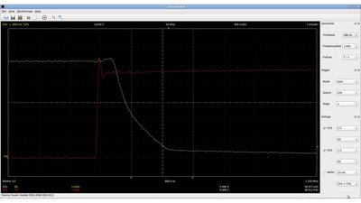
Switching transistors at their maximum frequency is tricky! At the oscillograph drawn above you can see the input curve (red) and the accordant output signal between the source drain line of an IRLZ24N (yellow). A 1kΩ resistor is switched in series to the gate pin simulating an input signal with a high inner resistance resulting in a worse slew rate of the MOSFET. You might also recognize that the input signal is not perfect. It's oscillating around it's maximum value while it is changing from 0V to 5V. There is always some kind of feedback between the signal source and the amplifying circuit like demonstrated at the previous chapter. Just remember the capacitance of a FETs gate area! Let's have a look at the power dissipated by the emitter collector line while the state alters from "on" to "off", meaning the resistance of the emitter collector line rises from it's minimum to its maximum. The current running through the output circuit is: The voltage drop at the transistor is: UTotal * RTransistor / (RTransistor + RLoad) The power dissipated by the emitter collector line is: or short: The maximum collector current of the BD135 is 1.5A, the maximum emitter collector voltage is 45V and the maximum power dissipation is 8W. So it looks like there is no problem in switching a 30Ω load connected to a 40V power supply. While altering the switching state from on to off, the resistance of the transistor is around 10Ω for a short span of time. By inserting those values at the equation above we get 10W! That's no problem, as long as the switching frequency is low. ConclusionNo input power is required to keep the switching state of a field effect transistor. A current is running for a short span of time while the state is altered. The higher the switching frequency, the higher the input power required to control the FET.Note the maximum emitter collector (source drain) voltage while switching inductive loads, because it might exceed the supply voltage clearly! Use a preferably high input voltage when switching power devices to "on" to keep the emitter collector (source drain) resistance low. Operating a transistor as an electric switch is often called digital amplification. <<< Amplifier Operational amplifier >>> News The Project Technology RoboSpatium Contribute Subject index Archives Download Responses Games Links Gadgets Contact Imprint |
|
|