|
|
|
|
News The Project Technology RoboSpatium Contribute Subject index Download Responses Games Gadgets Contact <<< Bipolar junction transistor (properties) Java-Applet JFETs >>> JFETsThe video about JFETsDesign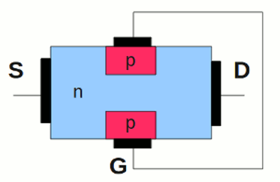
JFETs are controlled by three pins: Source (S), Drain (D) and Gate (G). At this drawing the source and drain pin are attached to the n-doped matrix of the crystal. The two p-doped regions are connected to the gate pin. There is just a small channel of n-doped material between the two p-doped regions. This is a picture of an n-channel JFET. 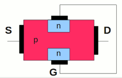
If the matrix consists of p-doped material with an n-doped gate region, the device is called p-channel JFET. 
Circuit symbol with labeled pins. Functionality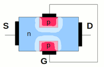
There are two pn junctions inside of the n-channel JFET shown at this drawing. The functionality of a single pn junction has been treated at the chapter semiconductor diodes. If no voltage is attached to the pins, a depletion layer, meaning an area with no movable charges (electrons, holes), is created around the two junctions. The depletion layers border a narrow channel of n-doped material at the middle of the transistor. 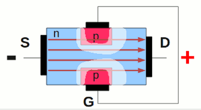
What happens if a positive voltage is applied between source and drain? Because of the electric field caused by the voltage source, the depletion layer is modified. There are more electrons located at the left side (Source) of the crystal than at the right side. Hence the depletion layer gets weakened at the left side while it is enforced at the right side. 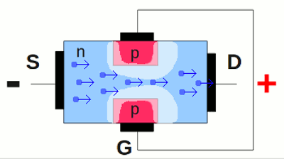
Still there is a narrow channel between the two p-doped region, enabling the electrons to drift from the source to the drain. Even without a voltage applied to the gate pin, an electric current is running through the transistor. JFETs are self conducting, bipolar junction transistors are self locking. 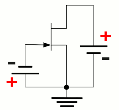
To cut off those current, the depletion layer has to be widened, so that the electrons are pushed out of the channel. Like explained at the chapter about semiconductor diodes, the pn junction has to be reverse biased to enlarge the depletion layer, hence the negative terminal has to be attached to the p-doped region, while the positive terminal has to be attached to the n-doped region. Source and drain are connected to another voltage source with the negative terminal attached to the source and the positive terminal attached to the drain. The source pin is connected to both voltage sources, hence it is the reference point (ground). 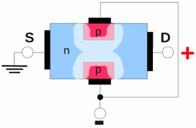
If a negative voltage is attached between source and drain pin, the depletion layer grows by what the resistance of the source drain line is increasing. If a certain voltage drop is reached, the electric current gets switched off completely. Only for a short span of time, a current is running through the gate pin while the voltage is altered. As soon as an equilibrium is established, no electric energy is needed to keep those condition. The resistance of the source drain line is solely caused by the electric fields of the pn junctions. JFET means Junction Field Effect Transistor. In contrast the resistance of bipolar junction transistors is caused by a current, which is why electric energy is required to keep the state of equilibrium. 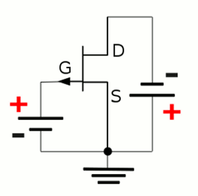
A positive voltage drop has to be attached between source and drain to cut off the current running through a p-channel JFET. 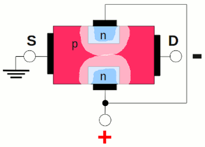
The polarity of the voltage sources has to be altered in comparison to an n-channel JFET. <<< Bipolar junction transistor (properties) Java-Applet JFETs >>> News The Project Technology RoboSpatium Contribute Subject index Archives Download Responses Games Links Gadgets Contact Imprint |
|
|